Printed wiring board, printed circuit board, and printed circuit board manufacturing method

Active Publication Date: 2014-02-13
CANON KK
View PDF6 Cites 10 Cited by
  • Summary
  • Abstract
  • Description
  • Claims
  • Application Information

AI Technical Summary

Benefits of technology

[0009]Accordingly, it is an object of the present invention to provide a printed wiring board, a printed ci

Problems solved by technology

Further, an insulator used for the printed wiring board has a thermal conductivity which is lower than that of the conductor pattern, and thus, the conductor pattern is liable to store heat.
By the way, in a reflow step of soldering the heat sink and the conductor pattern on the mounting surface, if molten solder is dr

Method used


Image

  • Printed wiring board, printed circuit board, and printed circuit board manufacturing method
  • Printed wiring board, printed circuit board, and printed circuit board manufacturing method
  • Printed wiring board, printed circuit board, and printed circuit board manufacturing method

Examples


Example

First Embodiment

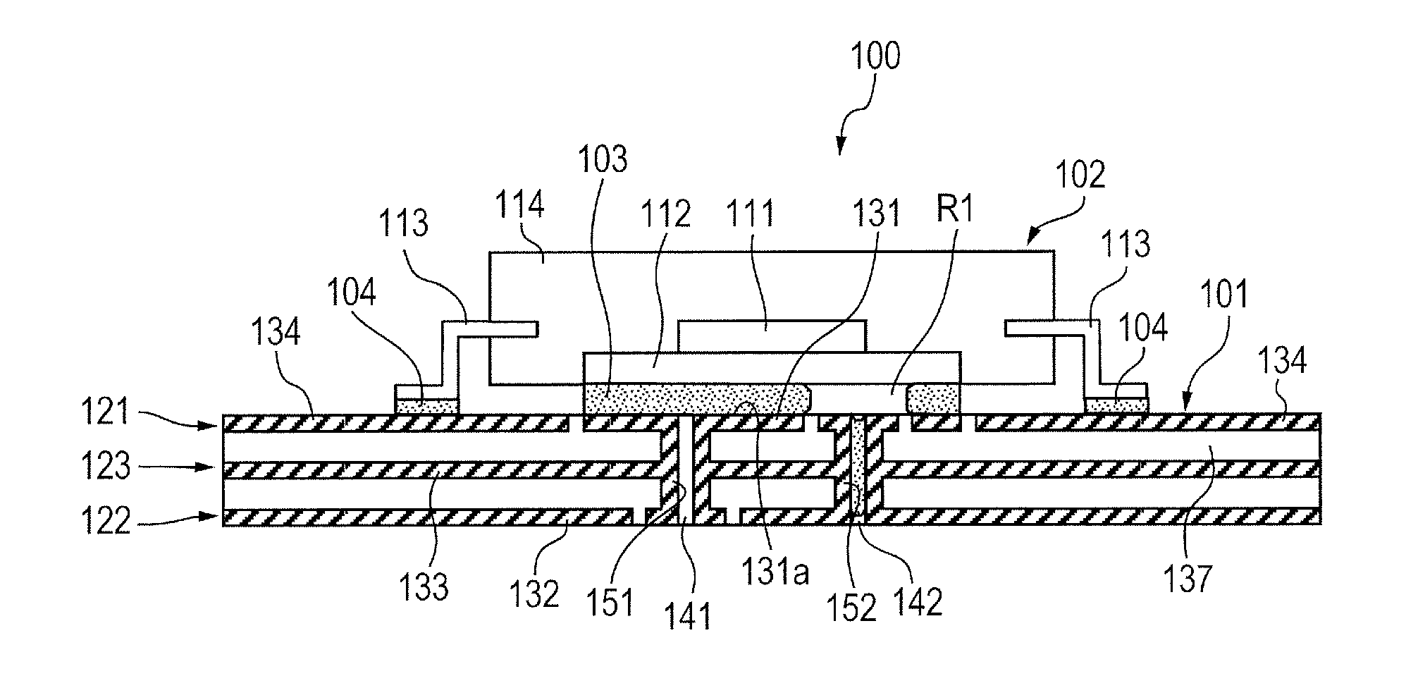
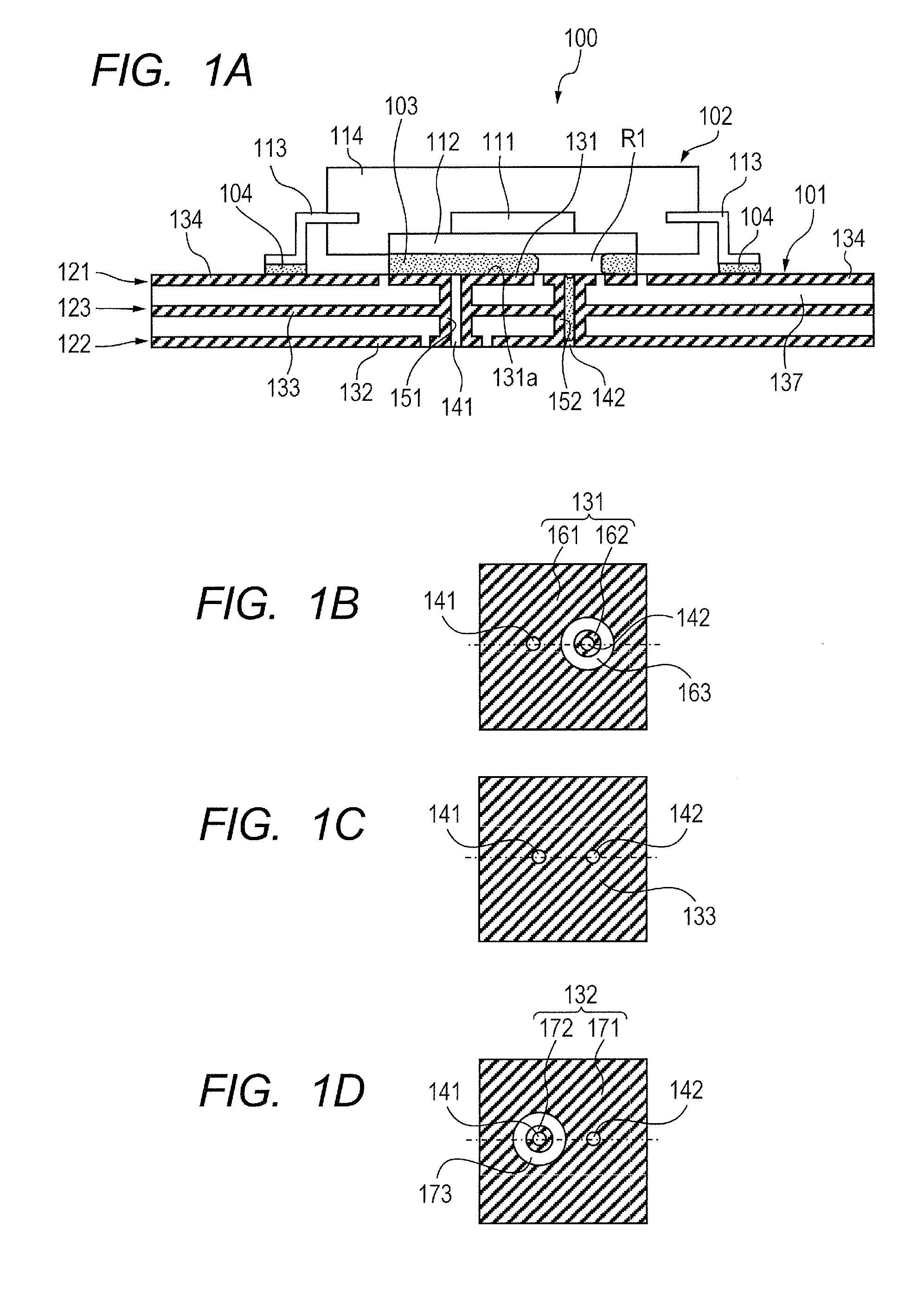
[0020]FIGS. 1A to 1D are explanatory diagrams illustrating a schematic structure of a printed circuit board according to a first embodiment of the present invention. FIG. 1A is a sectional view of the printed circuit board, FIG. 1B is a plan view of a first conductor pattern of a printed wiring board, FIG. 1C is a plan view of an inner layer conductor pattern of the printed wiring board, and FIG. 1D is a plan view of a second conductor pattern of the printed wiring board.

[0021]As illustrated in FIG. 1A, a printed circuit board 100 includes a printed wiring board 101 and a semiconductor package 102 mounted on the printed wiring board 101. In the first embodiment, the semiconductor package 102 is a QFP, QFN, or BGA semiconductor package. In FIGS. 1A to 1D, the semiconductor package 102 is illustrated as a QFP semiconductor package.

[0022]The semiconductor package 102 includes a die 111 which is a semiconductor element and a heat source, a heat sink 112 which is thermall...

Example

Second Embodiment

[0055]Next, a printed circuit board according to a second embodiment of the present invention is described.

[0056]FIGS. 3A to 3D are explanatory diagrams illustrating a schematic structure of the printed circuit board according to the second embodiment of the present invention. FIG. 3A is a sectional view of the printed circuit board, FIG. 3B is a plan view of a first conductor pattern of the printed wiring board, FIG. 3C is a plan view of an inner layer conductor pattern of the printed wiring board, and FIG. 3D is a plan view of a second conductor pattern of the printed wiring board.

[0057]As illustrated in FIG. 3A, a printed circuit board 200 includes a printed wiring board 201 and a semiconductor package 102 which is similar to that according to the first embodiment and mounted on the printed wiring board 201.

[0058]The printed wiring board 201 is a three-layer printed wiring board in which a surface layer 221 which is a first surface layer on which the semiconducto...

Example

Third Embodiment

[0082]Next, a printed circuit board according to a third embodiment of the present invention is described. FIGS. 4A to 4C are explanatory diagrams illustrating a schematic structure of the printed circuit board according to the third embodiment of the present invention. FIG. 4A is a plan view of a first conductor pattern of a printed wiring board, FIG. 4B is a plan view of an inner layer conductor pattern of the printed wiring board, and FIG. 4C is a plan view of a second conductor pattern of the printed wiring board.

[0083]In the above-mentioned first embodiment, a case is described in which the clearance 163 corresponding to the through hole 142 is circular and the clearance 173 corresponding to the through hole 141 is circular, but the present invention is not limited thereto. As in the third embodiment, square clearances 363 and 373 illustrated in FIGS. 4A and 4C may be included. Specifically, it is enough that the clearances divide the plane-like conductive patte...


PUM

PropertyMeasurementUnit
Electrical conductoraaaaaaaaaa

Abstract

Provided is a printed wiring board including a first heat dissipation pattern placed in one surface layer on which a semiconductor package is to be mounted, a second heat dissipation pattern placed in the other surface layer, and an inner layer conductor pattern placed in an inner layer, in which through holes are formed in the printed wiring board; the first heat dissipation pattern has a joint portion which is placed in an opposed region opposed to a heat sink of the semiconductor package and which is joined to the heat sink with solder; at least one of the through holes is placed in the opposed region; and the second heat dissipation pattern is formed in a pattern in which an end portion of a conductor film in the one of the through holes on the other surface layer side is separated.

Description

BACKGROUND OF THE INVENTION[0001]1. Field of the Invention[0002]The present invention relates to a printed wiring board having a semiconductor package including a heat sink mounted thereon, a printed circuit board including the printed wiring board, and a printed circuit board manufacturing method.[0003]2. Description of the Related Art[0004]In a semiconductor package such as an IC which is mounted on a printed wiring board, a heat sink for dissipating generated heat is provided on a rear surface of a semiconductor package body. This is because, in recent years, as signal processing in a semiconductor package becomes faster, heat generated in the semiconductor package tends to increase, and it is necessary to efficiently dissipate heat in the semiconductor package. Japanese Patent Application Laid-Open No. 2006-80168 discloses a printed wiring board in which, for the purpose of efficiently dissipating heat generated in such a semiconductor package, a heat sink of the semiconductor p...

Claims


Application Information

Patent Timeline
IPC IPC(8): H05K1/02H05K13/04
CPCH05K13/0465H05K1/0271H05K1/0207H05K1/113H05K2201/09772
Inventor OHIRA, MASAHARU
Owner CANON KK
Why Eureka
Try Eureka