Reduction of Proximity Effects in Field-Effect Transistors with Embedded Silicon-Germanium Source and Drain Regions

Inactive Publication Date: 2014-02-27
TEXAS INSTR INC
View PDF4 Cites 9 Cited by
  • Summary
  • Abstract
  • Description
  • Claims
  • Application Information

AI Technical Summary

Benefits of technology

[0016]Embodiments of this invention provide an integrated circuit and method of fabricating the same having metal-oxide-semiconductor (MOS) transistors with embedde

Problems solved by technology

This weaker p-channel MOS performance can be a limiting factor in CMOS switching speed.
This strain relaxation is detrimental in that it reduces the effectiveness of the SiGe structures in improving carrier mobi

Method used


Image

  • Reduction of Proximity Effects in Field-Effect Transistors with Embedded Silicon-Germanium Source and Drain Regions
  • Reduction of Proximity Effects in Field-Effect Transistors with Embedded Silicon-Germanium Source and Drain Regions
  • Reduction of Proximity Effects in Field-Effect Transistors with Embedded Silicon-Germanium Source and Drain Regions

Examples


Example

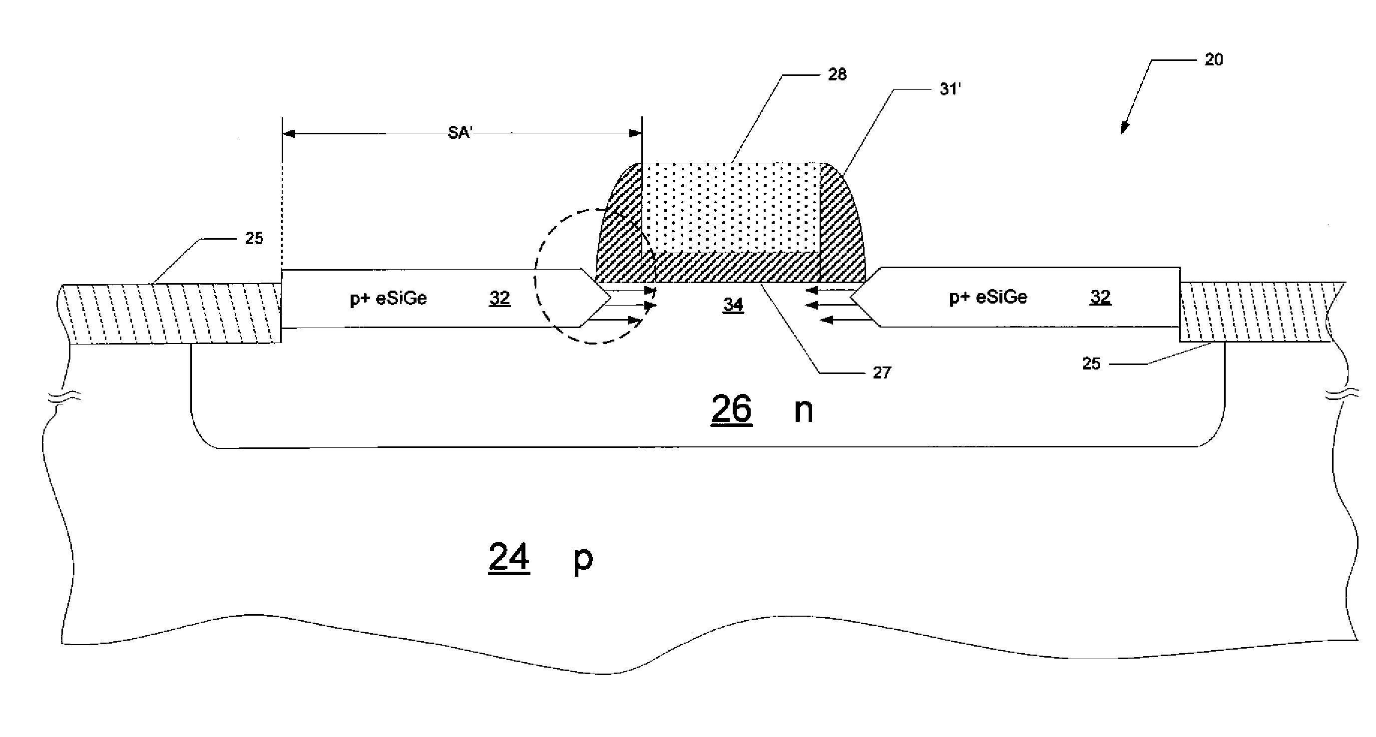
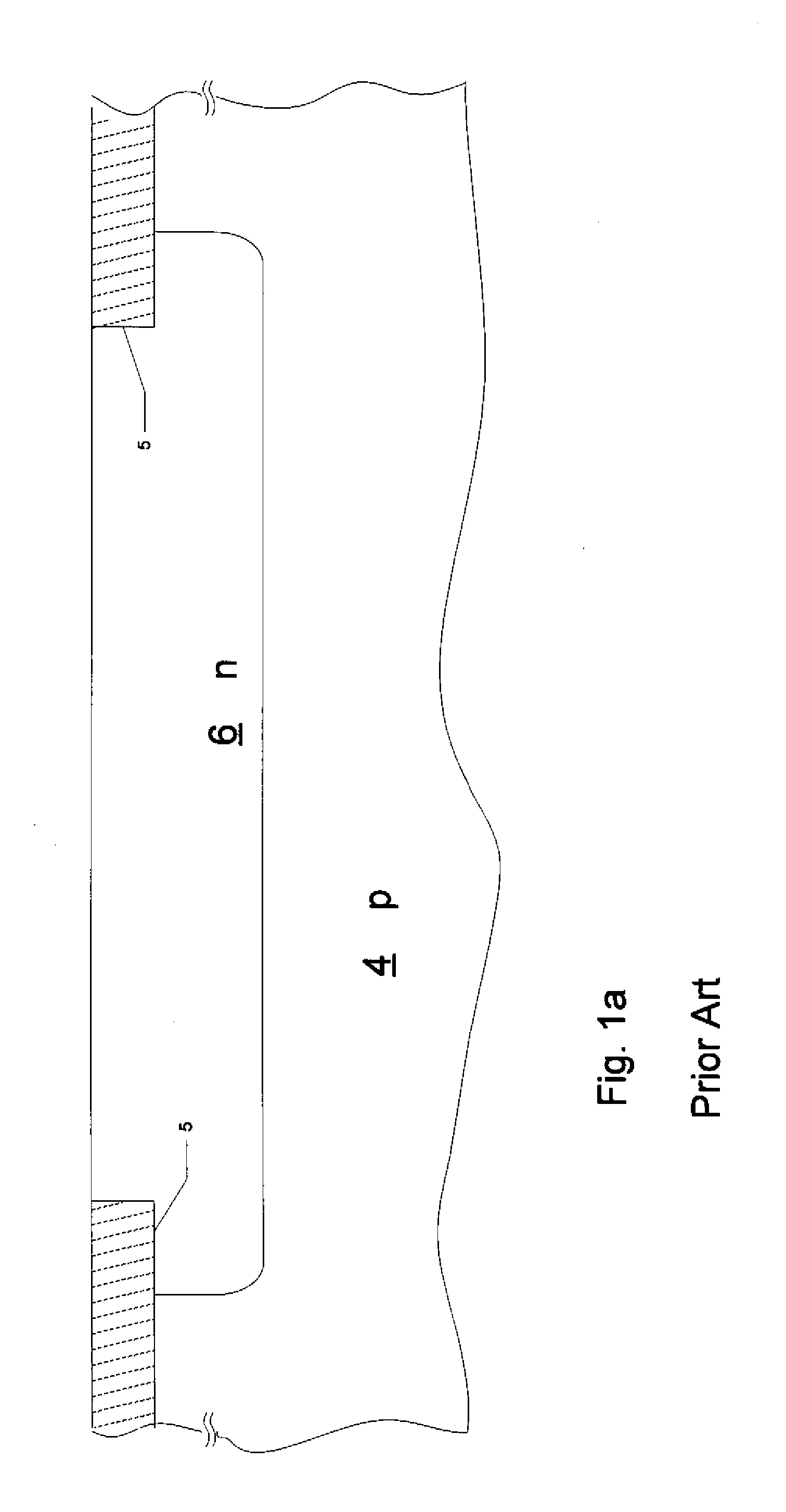
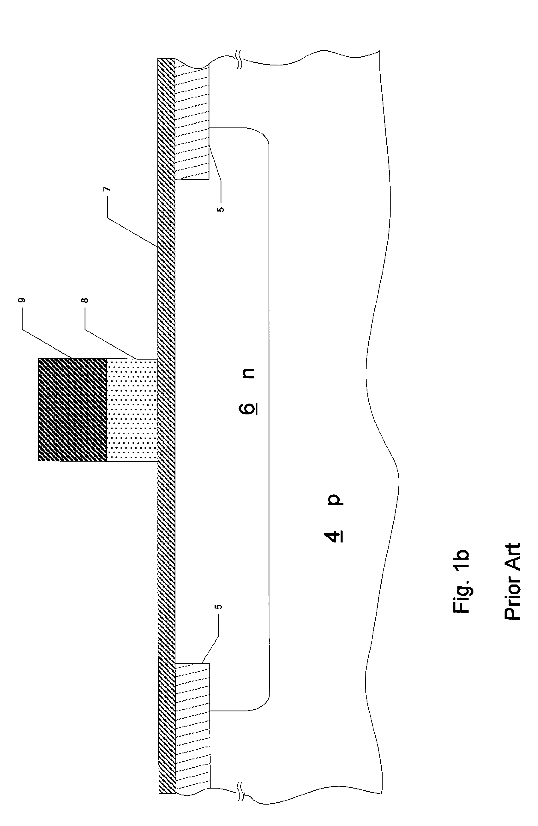
[0029]This invention will be described in connection with certain embodiments, namely as implemented into an integrated circuit fabricated according to a metal-oxide-semiconductor (MOS) technology as applied to planar p-channel MOS transistors formed in bulk silicon, as it is contemplated that this invention is especially beneficial in such an application. However, it is also contemplated that this invention may be used in other types of integrated circuits, including n-channel MOS transistors, complementary MOS (CMOS) integrated circuits, integrated circuits fabricated in silicon-on-insulator (SOI) structures, non-planar transistors, other types of field-effect transistors, and the like. Accordingly, it is to be understood that the following description is provided by way of example only, and is not intended to limit the true scope of this invention as claimed.

[0030]FIGS. 3a and 3b illustrate, in cross-section, the construction of p-channel MOS transistor 20 according to an embodim...


PUM


Abstract

An integrated circuit and method of fabricating the same utilizing embedded silicon-germanium (SiGe) source/drain regions, and in which the proximity effect of nearby shallow trench isolation structures is reduced. Embedded SiGe source/drain structures are formed by selective epitaxy into recesses etched into the semiconductor surface, on either side of each gate electrode. The SiGe structures overfill the recesses by at least about 30% of the depth of the recesses, as measured from the interface between the channel region and the overlying gate dielectric at the edge of the gate electrode. This overfill has been observed to reduce proximity effects of nearby shallow trench isolation structures on nearby transistors. Additional reduction in the proximity effect can be obtained by ensuring sufficient spacing between the edge of the gate electrode and a parallel edge of the nearest shallow trench isolation structure.

Description

CROSS-REFERENCE TO RELATED APPLICATIONS[0001]Not applicable.STATEMENT REGARDING FEDERALLY SPONSORED RESEARCH OR DEVELOPMENT[0002]Not applicable.BACKGROUND OF THE INVENTION[0003]This invention is in the field of integrated circuit manufacture. Embodiments of this invention are more specifically directed to metal-oxide-semiconductor field-effect transistors (MOSFETs) to which strain engineering technology is applied.[0004]Recent advances in semiconductor technology as applied to integrated circuits include the use of “strain engineering” (or, alternatively, “stress engineering”) in the manufacture of semiconductor device structures. As is fundamental in MOS device technology, the source / drain current (i.e., drive) of a MOS transistor in both the triode and saturation regions is proportional to carrier mobility in the channel region. It has been discovered that the tuning of strain in the crystal lattice of metal-oxide-semiconductor (MOS) transistor channel regions can enhance carrier ...

Claims


Application Information

Patent Timeline
IPC IPC(8): H01L21/336H01L29/78
CPCH01L29/165H01L29/665H01L29/66636H01L29/7848
Inventor CHOI, YOUN SUNGRILEY, DEBORAHEKBOTE, SHASHANK SURESHCHANDRA
Owner TEXAS INSTR INC
Why Eureka
Try Eureka