Metal/ceramic bonding substrate and method for producing same

a technology of metal/ceramic bonding and substrate, which is applied in the direction of printed circuit aspects, transportation and packaging, chemistry apparatus and processes, etc., can solve the problems of warpage of the substrate, increase of the temperature of the substrate, and increase of the heat sink characteristic of the base plate, so as to prevent the diffusion of metal and al. , the effect of increasing the thermal conductivity

Active Publication Date: 2014-02-27
DOWA METALTECH CO LTD
View PDF19 Cites 4 Cited by
  • Summary
  • Abstract
  • Description
  • Claims
  • Application Information

AI Technical Summary

Benefits of technology

[0020]According to these aspects of the present invention, even if a base plate of aluminum or an aluminum alloy is formed so as to surround a metal plate of a metal, which has a higher thermal conductivity than that of aluminum or the aluminum alloy, when a metal / ceramic bonding substrate integrated with the base plate is produced by the molten metal bonding method, it is possible to produce the metal / ceramic bonding substrate which can prevent the formation of an intermetallic compound or solid solution of the metal and Al and which can prevent the diffusion of the metal and Al.

Problems solved by technology

Therefore, if the base plate warps during soldering, when the radiating fin or cooling jacket is mounted on the base plate, the clearance therebetween increases, so that the heat sink characteristic of the base plate extremely deteriorates.
In addition, even if a metal / ceramic bonding substrate substantially having no warpage is obtained, the warpage of the substrate increases if thermal shocks are repeatedly applied thereto.
However, the radiating performance of the circuit board disclosed in Japanese Patent Laid-Open No. 2001-7465 is deteriorated by the aluminum nitride substrate since the thermal conductivity thereof is lower than that of the radiating plate (metal base plate) of copper, aluminum or an alloy thereof although the aluminum nitride substrate has a high thermal conductivity (170 W / mK) as a ceramic substrate.
Even if a ceramic substrate having a thermal conductivity equal to or higher than that of the metal base plate can be used, such a ceramic substrate is very expensive, so that it is difficult to industrially mass-produce circuit boards using such very expensive ceramic substrates.
In addition, in order to bond the plurality of aluminum nitride substrates and the aluminum or aluminum alloy plates to each other to produce the multilayer structure and in order to bond the circuit plate of aluminum or the aluminum alloy and the radiating plate to the multilayer structure, it is required to apply very high pressures using the bonding material (brazing filler metal), and it is required to carry out a laminating step for producing the multilayer structure, so that the producing costs are high.
In addition, when the insulating circuit board disclosed in Japanese Patent Laid-Open No. 2003-86747 is produced, it is difficult to inject the molten metal of aluminum or the aluminum alloy into the mold at a high pressure while the ceramic plate is held at a predetermined position in the mold.
Therefore, there are some cases where it is not possible to bond the ceramic plates at appropriate positions, so that it is difficult to completely cover the second ceramic plate with the thermal diffusing plate and the radiating plate to precisely position the second ceramic plate.
For that reason, it is difficult to control the warpage of the insulating circuit board, so that there is the possibility that the reliability thereof may be deteriorated by the variation in warpage thereof.

Method used


Image

  • Metal/ceramic bonding substrate and method for producing same
  • Metal/ceramic bonding substrate and method for producing same
  • Metal/ceramic bonding substrate and method for producing same

Examples


first preferred embodiment

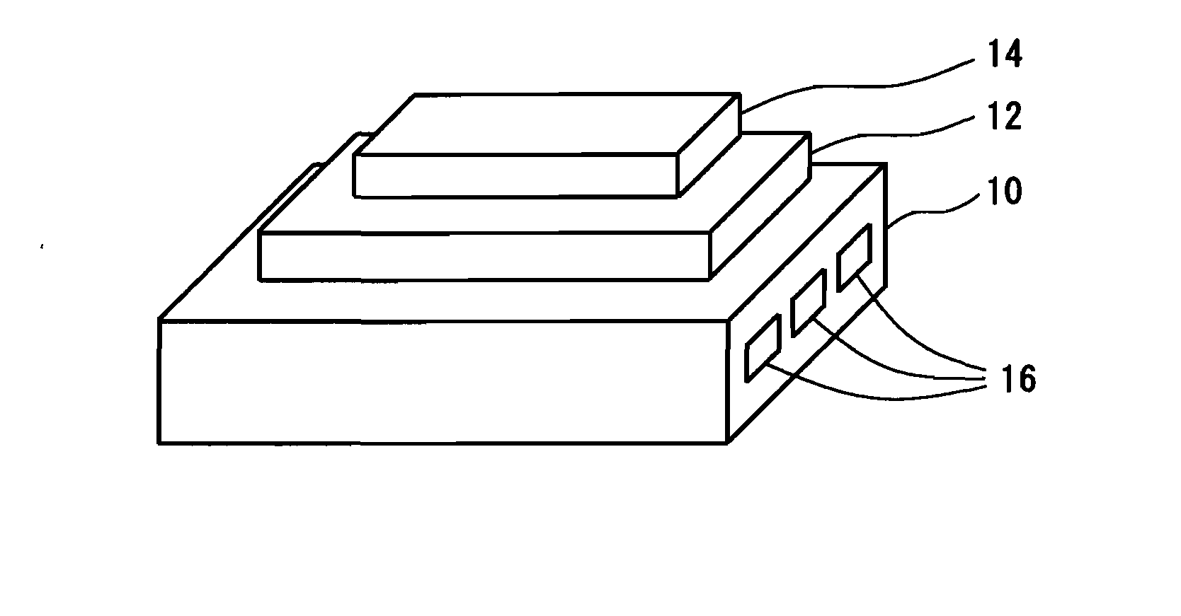
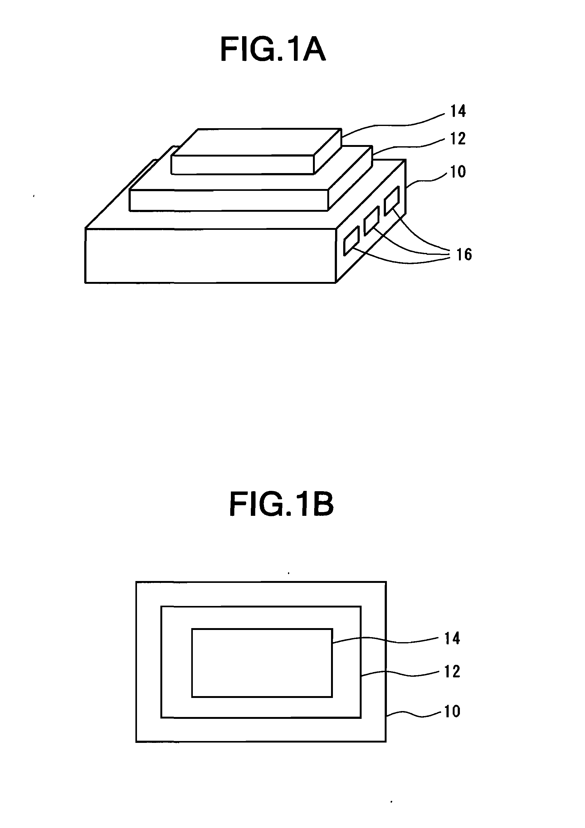
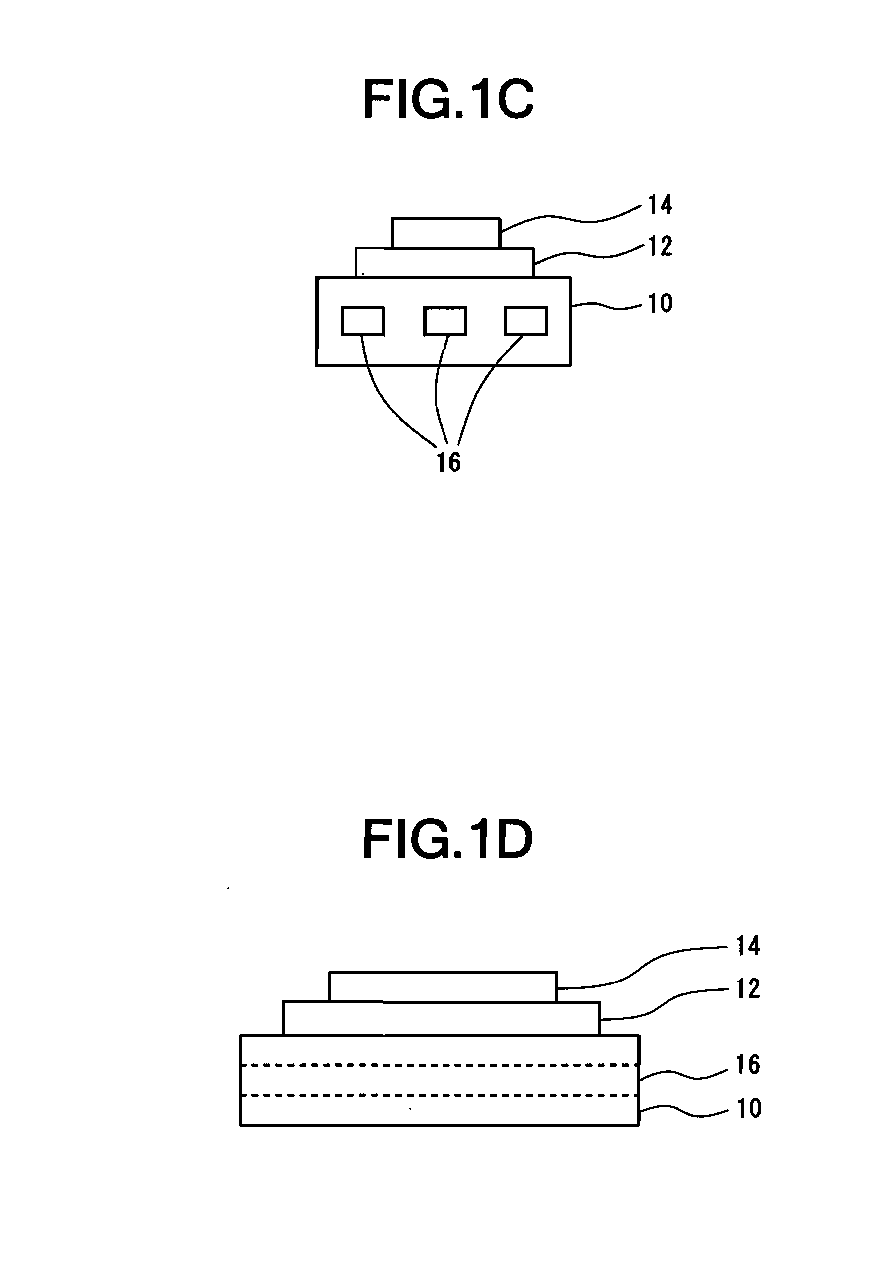
[0067]As shown in FIGS. 1A through 1D, the first preferred embodiment of a metal / ceramic bonding substrate according to the present invention comprises: a metal base plate 10 of a metal having a substantially rectangular planar shape; a ceramic substrate 12 having a substantially rectangular planar shape, one side of the ceramic substrate 12 being bonded directly to the metal base plate 10; and a circuit pattern forming metal plate 14 of a metal which has a substantially rectangular planar shape and which is bonded directly to the other side of the ceramic substrate 12.

[0068]As shown in FIGS. 1A, 1C and 1D, a plurality of reinforcing plate or rod members 16 of a metal (three elongated reinforcing plate members 16 having rectangular planar and sectional shapes in this preferred embodiment) pass through the interior of the metal base plate 10 from one of both end faces of the metal base plate 10 in longitudinal directions to the other end face thereof to extend in longitudinal directi...

example 1

[0083]First, there was prepared a mold of carbon having a similar shape to that of the mold 20 shown in FIGS. 2A through 2D, except that the bottom face of the metal base plate forming portion 22a has two ceramic substrate housing portions 22b spaced from each other and that the bottom face of each of the ceramic substrate housing portions 22b has a metal plate forming portion 22c. There were also prepared two ceramic substrates 12 of AlN having a size of 50 mm×50 mm×0.6 mm, and three reinforcing members 16 of 42 Alloy having a size of 150 mm×15 mm×0.6 mm. Then, the ceramic substrates 12 were arranged in the ceramic substrate housing portions 22b of the lower mold member 22 of the mold 20, respectively, and both end portions (portions having a length of 5 mm) of each of the reinforcing members 16 were arranged in the reinforcing member supporting portions 22d of the lower mold member 22, respectively. Thereafter, the lower mold member 22 was covered with the upper mold member 24 of ...

example 2

[0087]There was produced a metal / ceramic bonding substrate by the same method as that in Example 1, except that there were used a single reinforcing member 16 having a size of 150 mm×50 mm×1.0 mm and a mold 20 corresponding thereto.

[0088]With respect to the metal / ceramic bonding substrate thus obtained, the amount of warpage of the metal base plate 10 was measured by the same method as that in Example 1. As a result, the amount of warpage in longitudinal directions of the ceramic substrate 12 was +10 μm.

[0089]With respect to the metal / ceramic bonding substrate heated on a hot plate to cause the surface temperature of the substrate to be 260° C., the amount of warpage in longitudinal directions of the ceramic substrate 12 was measured. As a result, the amount of warpage in longitudinal directions of the ceramic substrate 12 was +298 μm.


PUM

PropertyMeasurementUnit
thicknessaaaaaaaaaa
temperatureaaaaaaaaaa
pressureaaaaaaaaaa

Abstract

A metal/ceramic bonding substrate includes: a ceramic substrate; a metal plate bonded directly to one side of the ceramic substrate; a metal base plate bonded directly to the other side of the ceramic substrate; and a reinforcing member having a higher strength than that of the metal base plate, the reinforcing member being arranged so as to extend from one of both end faces of the metal base plate to the other end face thereof without interrupting that the metal base plate extends between a bonded surface of the metal base plate to the ceramic substrate and the opposite surface thereof.

Description

TECHNICAL FIELD[0001]The present invention generally relates to a metal / ceramic bonding substrate and a method for producing the same. More specifically, the invention relates to a metal / ceramic bonding substrate wherein a metal plate (a metal circuit plate) for mounting electronic parts thereon is formed on one side of a ceramic substrate and wherein a metal base plate for heat radiation is formed on the other side thereof, and a method for producing the same.BACKGROUND ART[0002]In recent years, power modules are used for controlling heavy-current for electric vehicles, electric railcars and machine tools. In conventional power modules, a metal / ceramic insulating substrate is fixed to one side of a metal plate or compound material called base plate by soldering or the like, and semiconductor chips are fixed to a metal circuit plate of the ceramic insulating substrate by soldering. On the other side (reverse face) of the base plate, a radiating fin or cooling jacket of a metal is mo...

Claims


Application Information

Patent Timeline
Patent Type & Authority Applications(United States)
IPC IPC(8): H05K1/05B22D19/00B22D19/04
CPCH05K1/053B22D19/0081B22D19/04H05K1/0306H05K3/0061H05K3/022H05K2201/09136H05K2201/2009H05K2203/128H01L23/3735H01L21/4871H01L21/481H01L2924/0002Y10T428/24942Y10T428/12618Y10T428/2462Y10T428/2457H01L2924/00
Inventor OSANAI, HIDEYOTAKAHASHI, TAKAYUKIIDEGUCHI, SATORUKOTANI, HIROTAKA
Owner DOWA METALTECH CO LTD
Why Eureka
Try Eureka