Vertically Stacked Power FETS and Synchronous Buck Converter Having Low On-Resistance

a technology of synchronous buck converter and power fet, which is applied in the direction of semiconductor/solid-state device details, cooling/ventilation/heating modification, semiconductor devices, etc., can solve the problems of diminishing returns and achieve the effects of reducing power dissipation, improving efficiency, and increasing power density

Inactive Publication Date: 2014-03-06
TEXAS INSTR INC
View PDF3 Cites 53 Cited by
  • Summary
  • Abstract
  • Description
  • Claims
  • Application Information

AI Technical Summary

Benefits of technology

[0008]Applications of power electronics such as power converters, power blocks and power stages in markets as diverse as handheld, laptop, automotive, and medical products drive an ongoing demand for increased power density and reduced power dissipation. Applicants realized that these demands call for better efficiency and smaller packages. However, approaches to improve efficiency in DC / DC converters, which focus on reducing conduction losses in MOS FETs through lower drain-to-source on-resistance RDSon and lowering switching losses through low frequency operation, are on a point of diminishing returns, since low RDSon devices have large parasitic capacitances that do not facilitate the high-frequency operation required to improve power density.

Problems solved by technology

However, approaches to improve efficiency in DC / DC converters, which focus on reducing conduction losses in MOS FETs through lower drain-to-source on-resistance RDSon and lowering switching losses through low frequency operation, are on a point of diminishing returns, since low RDSon devices have large parasitic capacitances that do not facilitate the high-frequency operation required to improve power density.

Method used


Image

  • Vertically Stacked Power FETS and Synchronous Buck Converter Having Low On-Resistance
  • Vertically Stacked Power FETS and Synchronous Buck Converter Having Low On-Resistance
  • Vertically Stacked Power FETS and Synchronous Buck Converter Having Low On-Resistance

Examples


Embodiment Construction

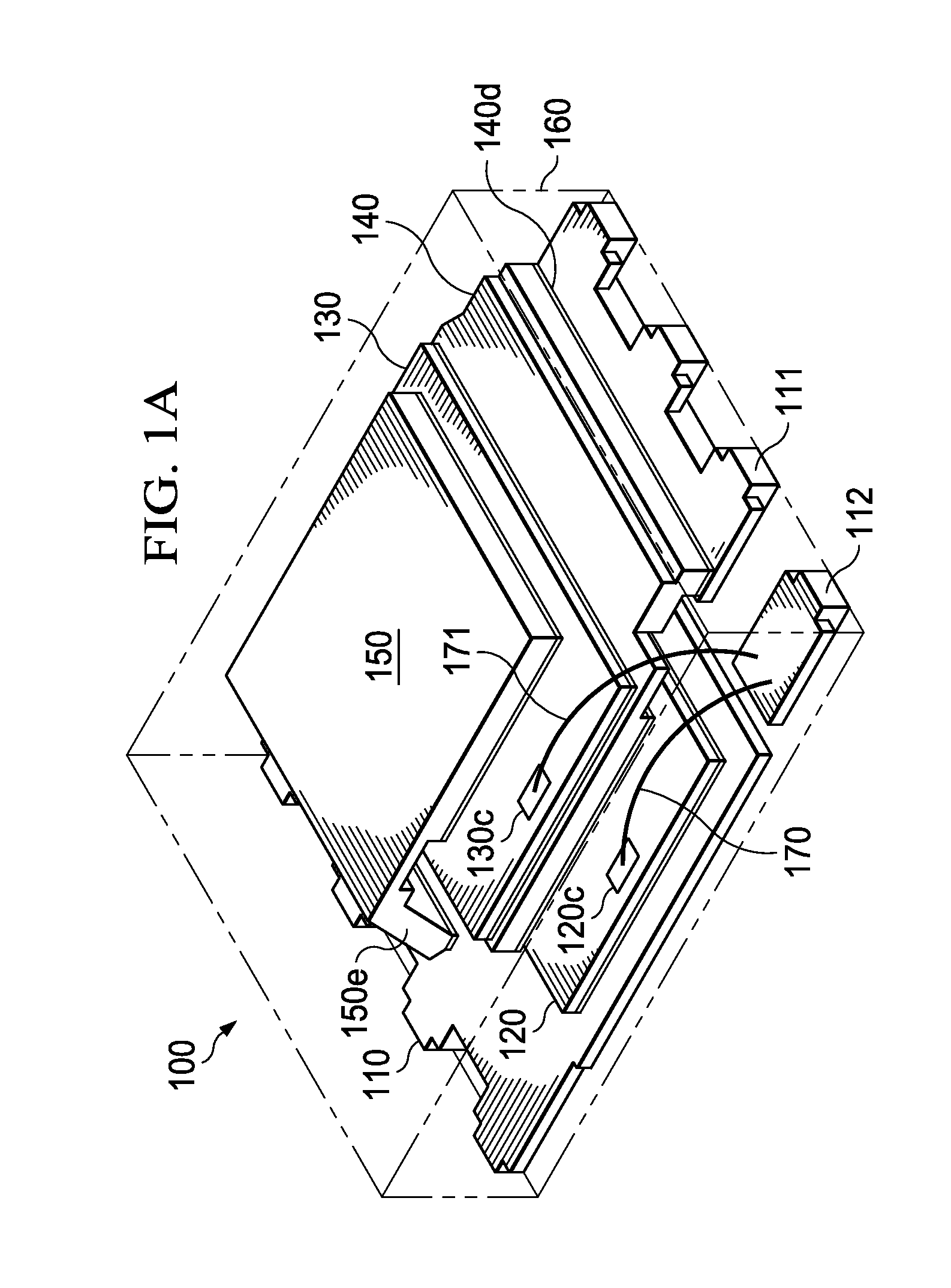
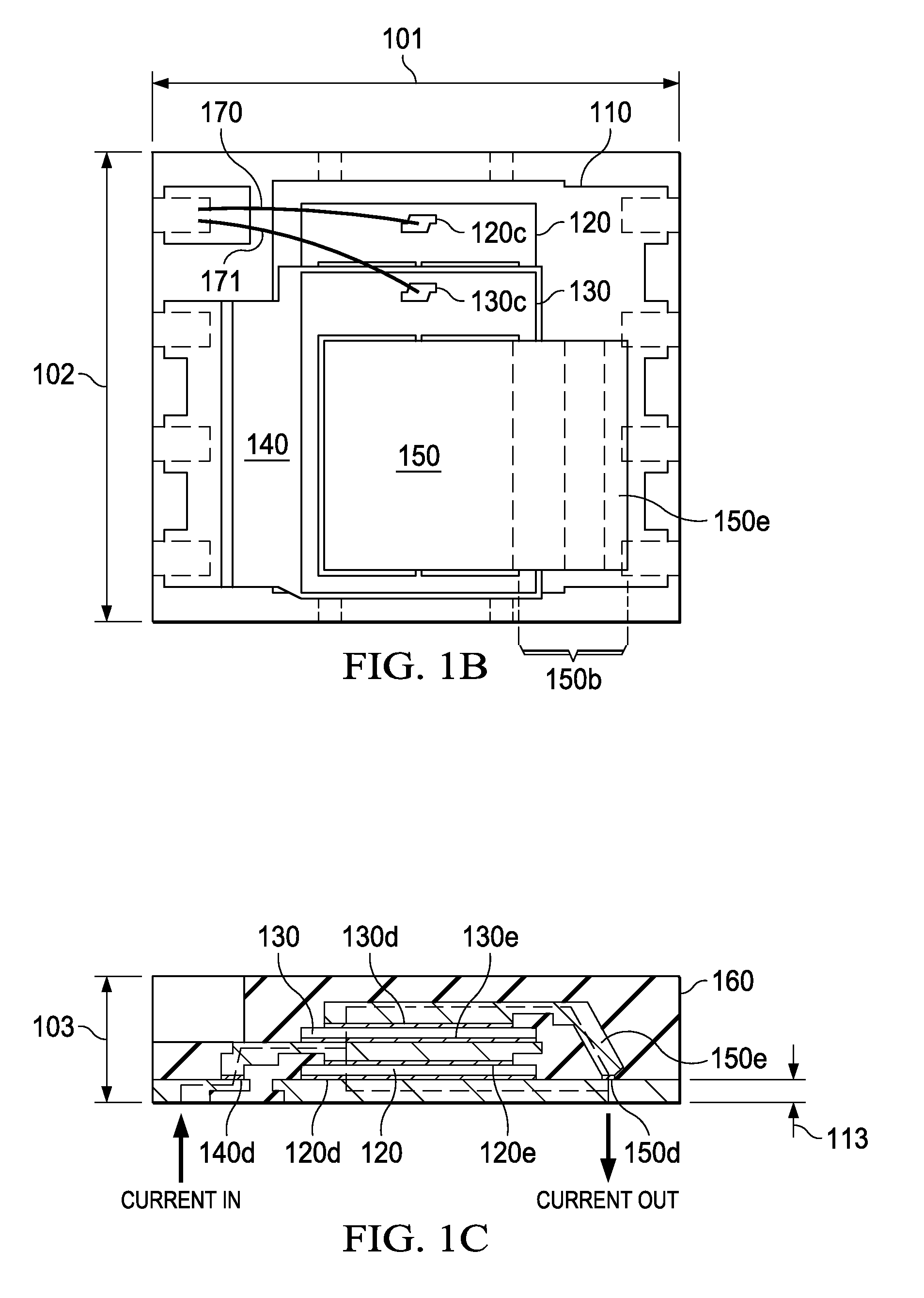
[0023]FIGS. 1A, 1B, and 1C display various views of an embodiment of an exemplary switch including a power field-effect transistor (FET), generally designated 100. Power FET 100 is assembled on a leadframe as a vertical stack of two FET chips according to the invention and encapsulated in packaging material 160 such as a molding compound; the encapsulation is assumed transparent in FIGS. 1A and 1B. The exemplary power FET of FIGS. 1A, 1B, and 1C has a length 101 of 6.0 mm, a width 102 of 5.0 mm, and a height 103 of 1.5 mm.

[0024]The leadframe includes a flat pad 110, a first flat lead 111, which is coplanar with pad 110, and a second flat lead 112, which is also coplanar with pad 110. The leadframe portions 110, 111, and 112 are preferably stamped or etched from a metallic starting sheet, hence the coplanarity. The leadframe is preferably made of copper or copper alloy; other alternatives include iron-nickel alloys (such as Alloy 42), aluminum, and Kovar™. Leadframe thickness 113 is ...


PUM


Abstract

A power FET (100) comprising a leadframe including a pad (110), a first lead (111), and a second lead (112); a first metal clip (150) including a plate (150a), an extension (150b) and a ridge (150c), the plate and extension spaced from the leadframe pad and the ridge connected to the pad; a vertically assembled stack of FET chips in the space between the plate and the pad, the stack including a first n-channel FET chip (120) having the drain terminal on one surface and the source and gate terminals on the opposite surface, the drain terminal attached to the pad, the source terminal attached to a second clip (140) tied to the first lead; and a second n-channel FET chip (130) having the source terminal on one surface and the drain and gate terminals on the opposite surface, the source terminal attached to the second clip, its drain terminal attached to the first clip; wherein the drain-source on-resistance of the FET stack is smaller than the on-resistance of the first FET chip and of the second FET chip.

Description

FIELD OF THE INVENTION[0001]The present invention is related in general to the field of semiconductor devices and processes, and more specifically to the structure and fabrication method of a small-size, three-dimensional field-effect transistors having ultra-low source-drain on-resistance.DESCRIPTION OF RELATED ART[0002]Among the popular families of power switching devices are the DC-DC power supply circuits, especially the category of Switched Mode Power Supply circuits. Particularly suitable for the emerging power delivery requirements are the synchronous Buck converters, or Power Blocks, with two power MOS field effect transistors (FETs) connected in series and coupled together by a common switch node. In the Power Block, the control FET chip, also called the high-side switch, is connected between the supply voltage VIN and the LC output filter, and the synchronous (sync) FET chip, also called the low side switch, is connected between the LC output filter and ground potential.[0...

Claims


Application Information

Patent Timeline
Patent Type & Authority Applications(United States)
IPC IPC(8): H05K7/20H01L25/07H05K1/18
CPCH01L23/4334H01L23/492H01L23/49537H01L23/49575H01L24/34H01L25/074H01L2224/37147H01L2224/40137H01L2224/48091H01L2224/49171H01L2224/48247H01L2224/49113H01L2924/1306H01L2924/13091H01L2924/00014H01L2924/00H01L2924/181H01L2224/40095H01L2224/40245H01L24/40H01L2224/73221H01L24/37H01L24/41H01L2224/83801H01L2224/84801H01L2224/0603H01L24/84H01L2924/00012H01L24/36
Inventor LOPEZ, OSVALDO JORGENOQUIL, JONATHAN A.HERBSOMMER, JUAN ALEJANDRO
Owner TEXAS INSTR INC
Why Eureka
Try Eureka