Replacement Metal Gate Process for CMOS Integrated Circuits

a technology of integrated circuits and metal oxides, which is applied in the direction of semiconductor devices, electrical equipment, transistors, etc., can solve the problems of cmos integrated circuits that complicate engineering, conventional gate dielectric layers, and oxides, and achieve good step coverage and fill characteristics

Active Publication Date: 2014-03-13
TEXAS INSTR INC
View PDF2 Cites 20 Cited by
  • Summary
  • Abstract
  • Description
  • Claims
  • Application Information

AI Technical Summary

Benefits of technology

[0018]Embodiments of this invention provide a high-k metal gate complementary metal-oxide-semiconductor (CMOS) structure and a method of manufacturing the same in which replacement metal gate structures are formed for both transistors with good step coverage and good fill characteristics.

Problems solved by technology

Conventional gate dielectric layers (e.g., silicon dioxide) have thus become extremely thin, which can be problematic from the standpoint of gate current leakage, manufacturing yield and reliability.
CMOS integrated circuits complicate this engineering, because the desired gate material work function is necessarily different for n-channel MOS transistors than for p-channel MOS transistors.
The provision of these different gate materials has resulted in structural issues in conventional CMOS integrated circuits, as will now be described in connection with FIGS. 1a through 1h.
As a result of this construction, gap 19 within the p-channel gate structure can be quite narrow, and thus difficult to fill with fill metal 18.
Such voids can result in increased resistivity in conduction along the gate electrode, and thus non-uniform potential along the gate electrode for individual transistors, and inconsistencies in operation among a population of transistors.
In addition, the formation of metal gate layers 15n, 15p adjacent to one another in the same gate structure raises the risk of interdiffusion of material between the two metals, particularly from the overlying metal gate layer 15n into the underlying metal gate layer 15p.
Such interdiffusion can change the work function of the intended gate metal (metal gate layer 15p in the example of FIG. 1h), and thus degrade the intended transistor performance.

Method used


Image

  • Replacement Metal Gate Process for CMOS Integrated Circuits
  • Replacement Metal Gate Process for CMOS Integrated Circuits
  • Replacement Metal Gate Process for CMOS Integrated Circuits

Examples


Embodiment Construction

[0026]This invention will be described in connection with its embodiments, namely as implemented into a complementary metal-oxide-semiconductor (CMOS) integrated circuit, as it is contemplated that the invention will be especially beneficial in such an application. However, it is further contemplated that this invention can be beneficially applied to other integrated circuit structures and processes. Accordingly, it is to be understood that the following description is provided by way of example only, and is not intended to limit the true scope of this invention as claimed.

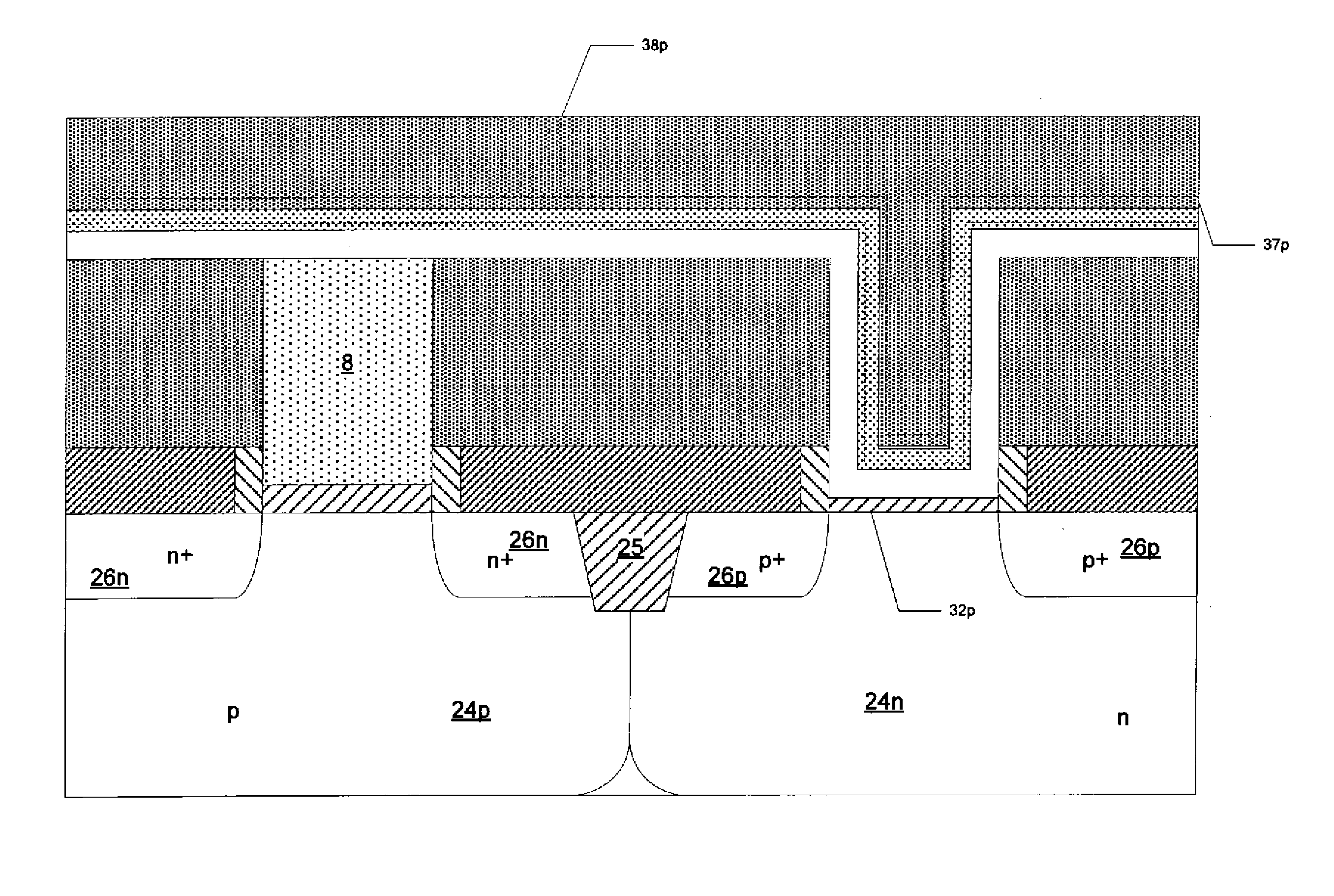
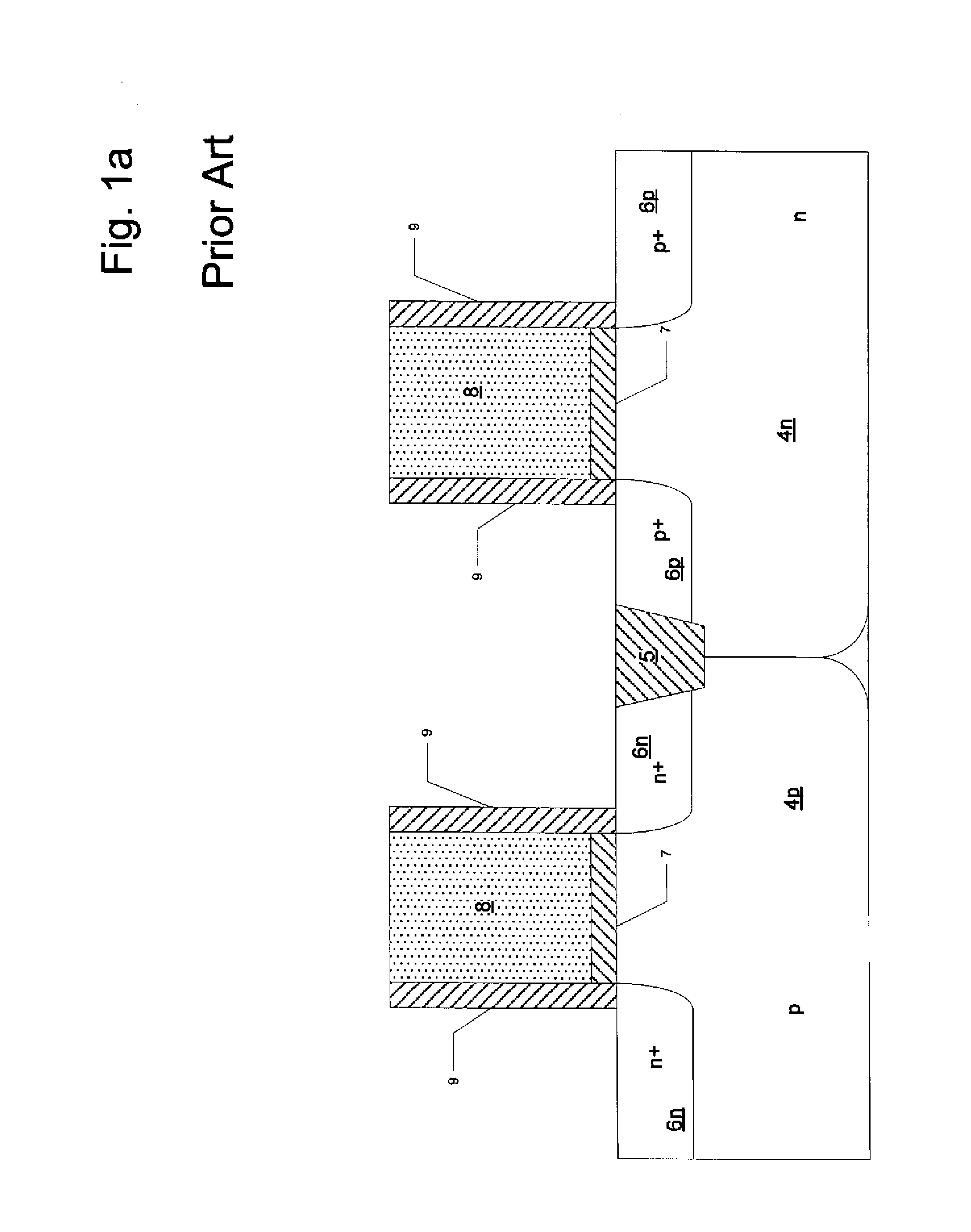
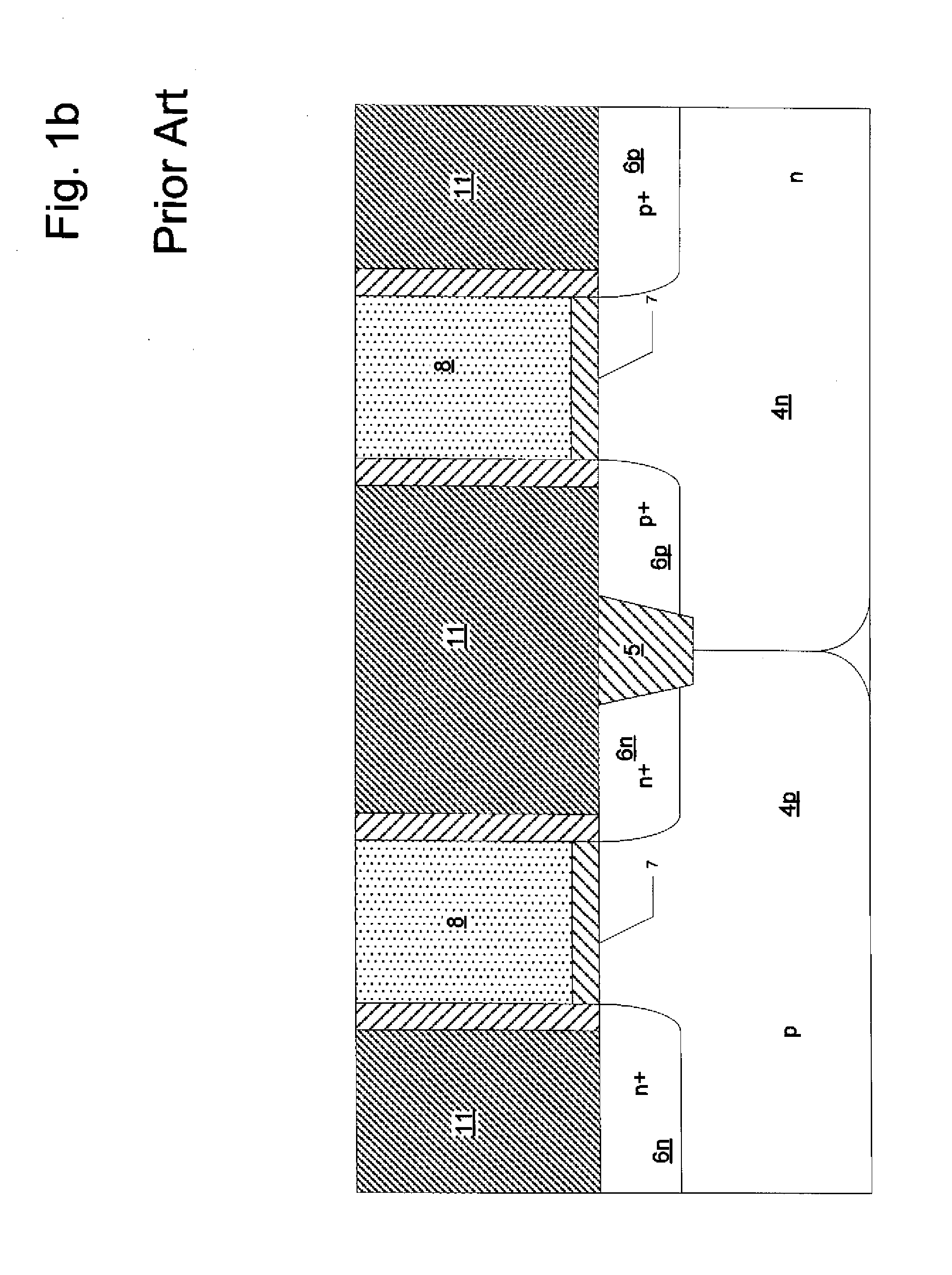
[0027]FIGS. 2a and 2b illustrate, in plan and cross-sectional views, respectively, the construction of p-channel MOS transistor 20p and n-channel MOS transistor 20n, both constructed in a CMOS integrated circuit according to embodiments of this invention. While these Figures show transistors 20n, 20p located adjacent to one another, it is of course contemplated that these transistors 20n, 20p may be located at a l...


PUM


Abstract

A complementary metal-oxide-semiconductor (CMOS) integrated circuit structure, and method of fabricating the same according to a replacement metal gate process. P-channel and n-channel MOS transistors are formed with high-k gate dielectric material that differ from one another in composition or thickness, and with interface dielectric material that differ from one another in composition or thickness. The described replacement gate process enables construction so that neither of the p-channel or n-channel transistor gate structures includes the metal gate material from the other transistor, thus facilitating reliable filling of the gate structures with fill metal.

Description

CROSS-REFERENCE TO RELATED APPLICATIONS[0001]Not applicable.STATEMENT REGARDING FEDERALLY SPONSORED RESEARCH OR DEVELOPMENT[0002]Not applicable.BACKGROUND OF THE INVENTION[0003]This invention is in the field of integrated circuit manufacture. Embodiments of this invention are more specifically directed to complementary metal-oxide-semiconductor (CMOS) integrated circuits having metal-gate transistors with high dielectric constant gate dielectrics.[0004]Many modern electronic devices and systems now include substantial computational capability for controlling and managing a wide range of functions and useful applications. As is fundamental in the art, reduction in the size of physical feature sizes of structures realizing transistors and other solid-state devices enables greater integration of more circuit functions per unit “chip” area, or conversely, smaller chip area consumed for a given circuit function. The capability of integrated circuits for a given cost has greatly increased...

Claims


Application Information

Patent Timeline
Patent Type & Authority Applications(United States)
IPC IPC(8): H01L21/8238H01L27/092
CPCH01L21/823842H01L21/823857H01L27/0922H01L27/092H01L27/0928H01L21/823814H01L21/823828
Inventor NIIMI, HIROAKISONG, SEUNG-CHUL
Owner TEXAS INSTR INC
Why Eureka
Try Eureka