

Method for forming insulation film having high density
- Summary
- Abstract
- Description
- Claims
- Application Information
AI Technical Summary
Benefits of technology
Problems solved by technology
Method used
Image

Examples
example 1
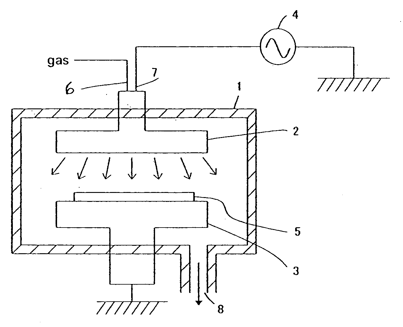
[0105]As a preliminary treatment (for improving padding property of an insulation film), a substrate was treated with a plasma using a plasma CVD apparatus shown in FIG. 1 under the following conditions:[0106]Susceptor temperature: 0° C.[0107]Auxiliary gas: He: 1000 sccm[0108]Reactor pressure: 1000 Pa[0109]27.12 MHz RF applied: 200 W
[0110]An insulation film was formed on a substrate using a plasma CVD apparatus shown in FIG. 1 under the following conditions, and the resultant thin film had the following properties:[0111]Susceptor temperature: 5° C.[0112]Source gas: TRES (triethoxysilane): 10 sccm[0113]Additive gas: Isopropyl alcohol: 150 sccm[0114]Oxidizing gas: O2: 50 sccm[0115]Inert gas: He: 630 sccm[0116]27 MHz RF applied: 200 W[0117]Reactor pressure: 266.6 Pa[0118]Space between the silicon substrate and the upper electrode: 10 mm[0119]Deposition rate: 49 nm / min
[0120]The thin film formed on the substrate was then cured using the furnace chamber under the following conditions, and...
example 2
[0129]As a preliminary treatment (for improving padding property of an insulation film), a substrate was treated with a plasma using a plasma CVD apparatus shown in FIG. 1 under the following conditions:[0130]Susceptor temperature: 0° C.[0131]Auxiliary gas: He: 1000 sccm[0132]Reactor pressure: 1000 Pa[0133]27.12 MHz RF applied: 200 W
[0134]An insulation film was formed on a substrate using a plasma CVD apparatus shown in FIG. 1 under the following conditions, and the resultant thin film had the following properties:[0135]Susceptor temperature: 0° C.[0136]Source gas: TRES (triethoxysilane): 10 sccm[0137]Additive gas: Isopropyl alcohol: 50 sccm[0138]Oxidizing gas: O2: 20 sccm[0139]Inert gas: He: 630 sccm[0140]27 MHz RF applied: 150 W[0141]Reactor pressure: 133.3 Pa[0142]Space between the silicon substrate and the upper electrode: 10 mm[0143]Deposition rate: 29 nm / min
[0144]The thin film formed on the substrate was then cured using the furnace chamber under the following conditions, and ...
example 3
[0153]As a preliminary treatment (for improving padding property of an insulation film), a substrate was treated with a plasma using a plasma CVD apparatus shown in FIG. 1 under the following conditions:[0154]Susceptor temperature: 0° C.[0155]Auxiliary gas: He: 1000 sccm[0156]Reactor pressure: 1000 Pa[0157]27.12 MHz RF applied: 200 W
[0158]An insulation film was formed on a substrate using a plasma CVD apparatus shown in FIG. 1 under the following conditions, and the resultant thin film had the following properties:[0159]Susceptor temperature: 0° C.[0160]Source gas: 1,1,3,3-tetradimethyldisilane: 10 sccm[0161]Additive gas: Isopropyl alcohol: 50 sccm[0162]Oxidizing gas: O2: 20 sccm[0163]Inert gas: He: 1200 sccm[0164]27 MHz RF applied: 100 W[0165]Reactor pressure: 266.6 Pa[0166]Space between the silicon substrate and the upper electrode: 10 mm[0167]Deposition rate: 70 nm / min[0168]The thin film formed on the substrate was then cured using the furnace chamber under the following conditio...
PUM
| Property | Measurement | Unit |
|---|---|---|
| Temperature | aaaaa | aaaaa |
| Temperature | aaaaa | aaaaa |
| Temperature | aaaaa | aaaaa |
Abstract
Description
Claims
Application Information