Method for manufacturing semiconductor device

Active Publication Date: 2005-10-04
PANNOVA SEMIC
View PDF4 Cites 10 Cited by
  • Summary
  • Abstract
  • Description
  • Claims
  • Application Information

AI Technical Summary

Benefits of technology

[0014]The present invention has been made to solve the aforementioned problem, and an object of the present invention is to realize metal intercon

Problems solved by technology

However, when miniaturization in the interconnect is further advanced, the known method for manufacturing a semicon

Method used


Image

  • Method for manufacturing semiconductor device
  • Method for manufacturing semiconductor device
  • Method for manufacturing semiconductor device

Examples


Embodiment Construction

[0037]An embodiment of the present invention will be described with reference to the drawings.

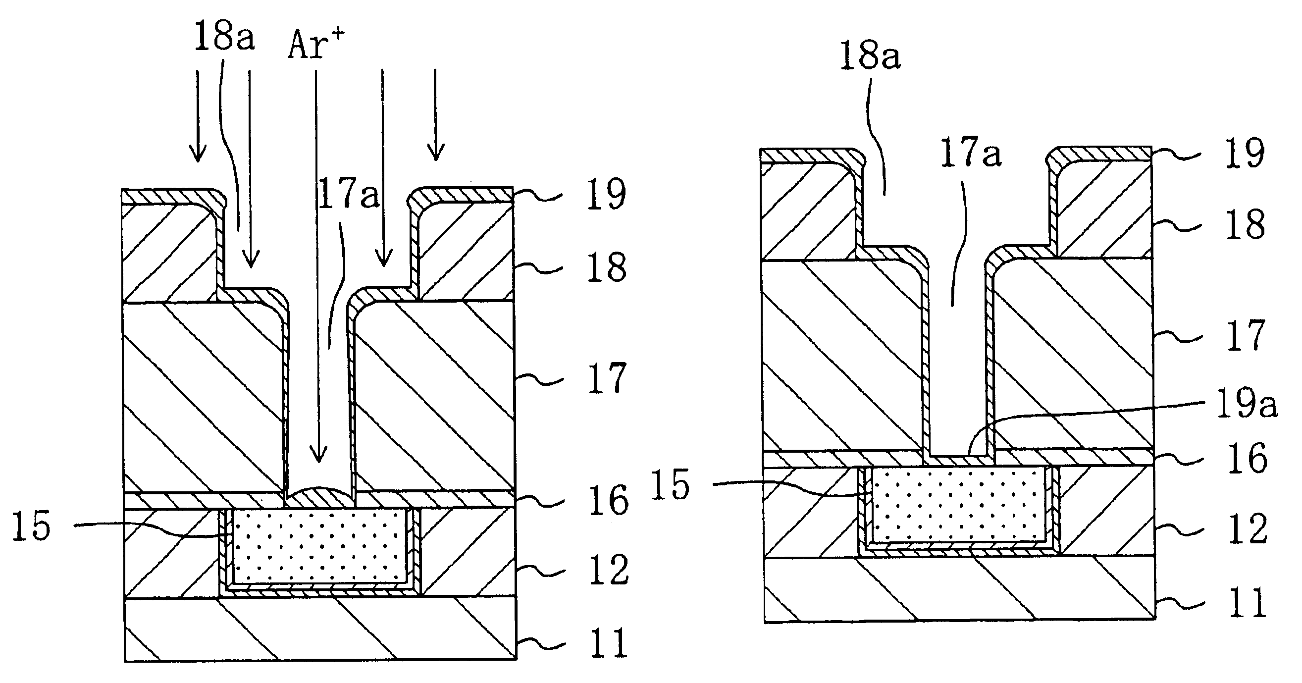
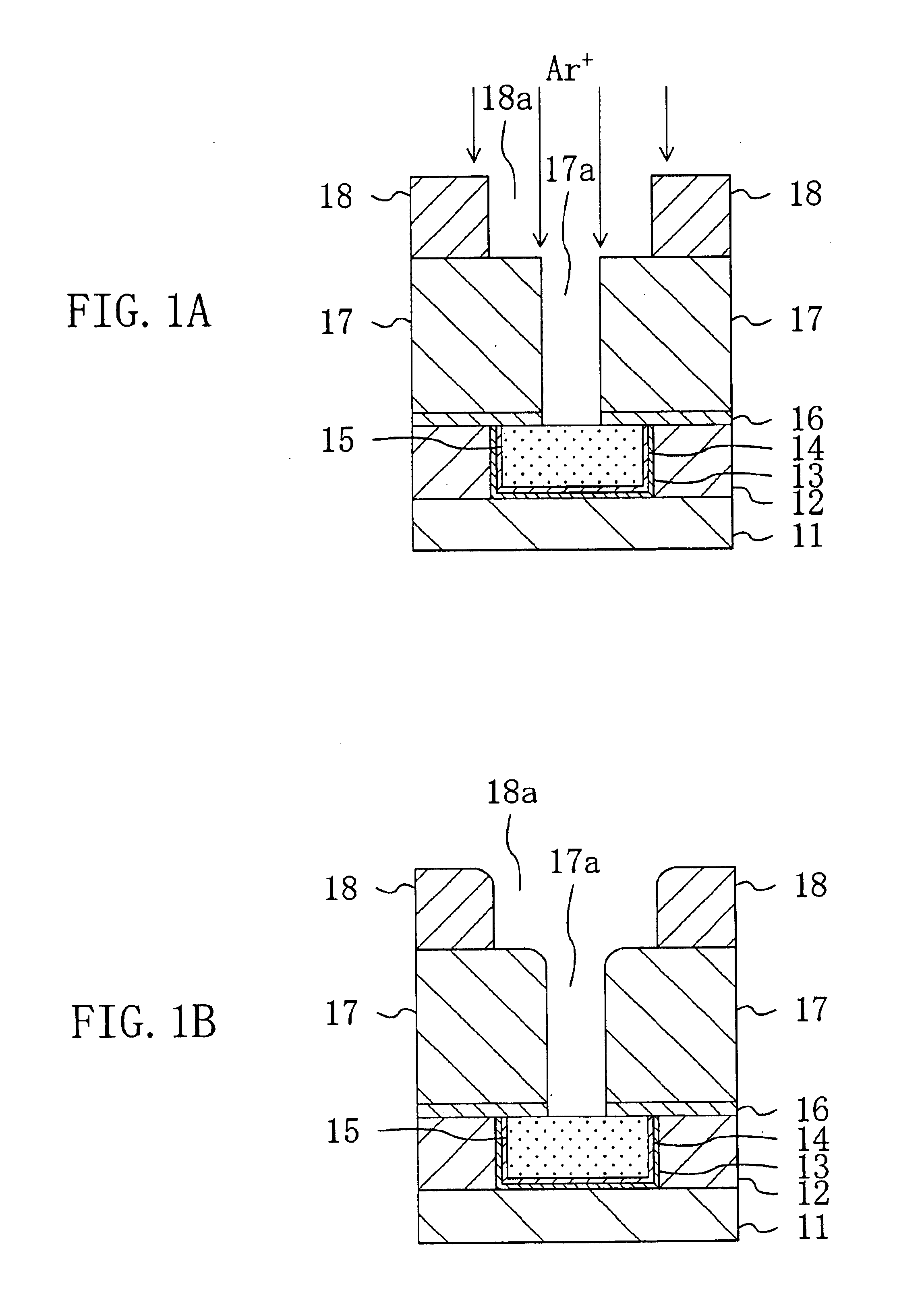
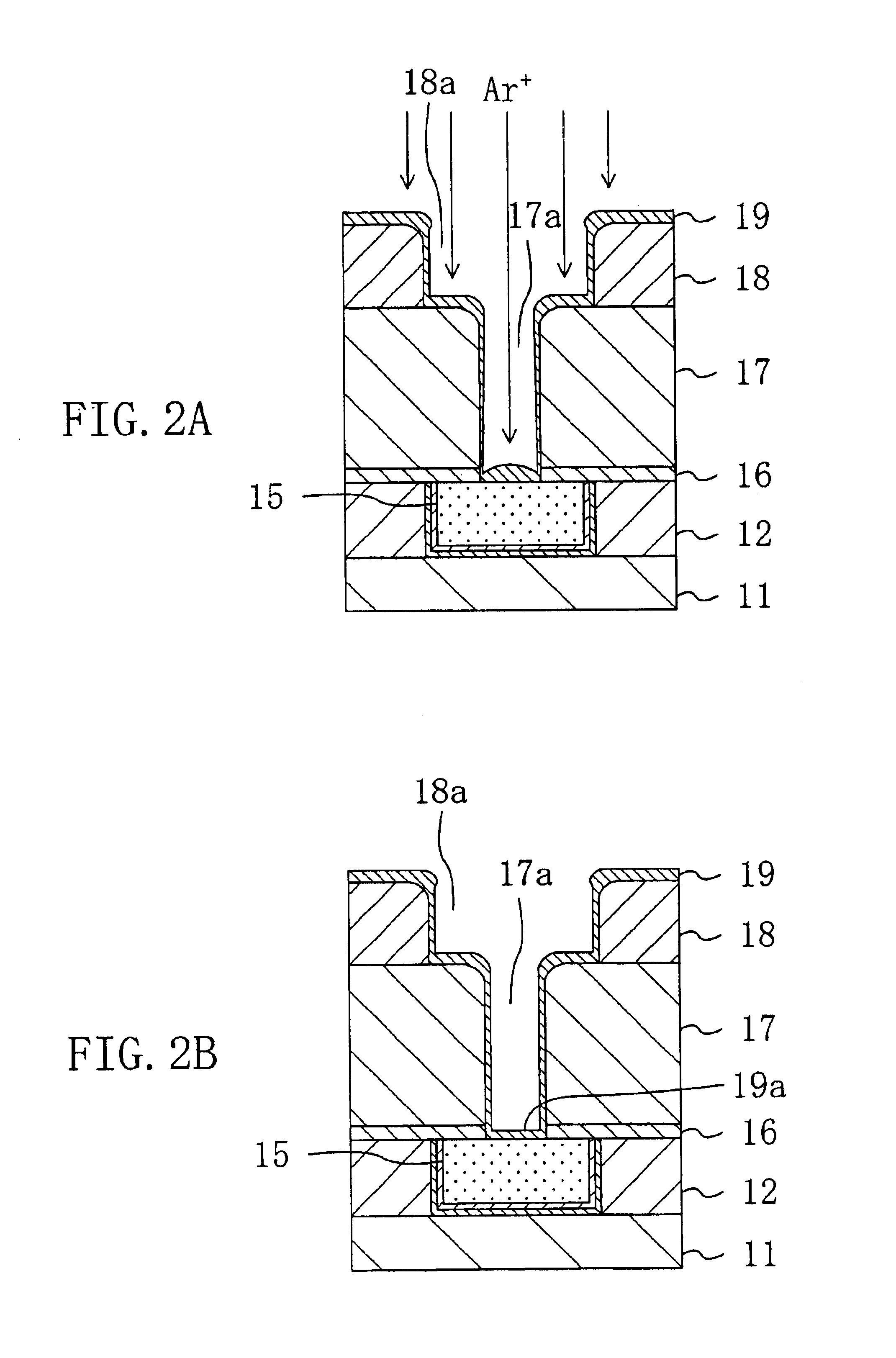
[0038]FIGS. 1A and 1B through 6A and 6B illustrate a method for manufacturing a semiconductor device according to an embodiment of the present invention, wherein cross-sectional structures of part of multilayer interconnects including a via hole (contact hole) are shown in the order of process steps.

[0039]Initially, as shown in FIG. 1A, for example, a first insulating film 11 and a second insulating film 12 which are each made of BPSG (Boron Phosphorous Silicate Glass) obtained by adding boron and phosphorous to silicon oxide are successively deposited on a semiconductor substrate (not shown) made of silicon (Si) by a chemical vapor deposition (CVD) process. Subsequently, a lower-interconnect-forming groove is formed in a predetermined region of the second insulating film 12 by lithography and dry etching. Thereafter, a lower barrier layer 13 made of tantalum nitride (TaN) and an upper barr...


PUM


Abstract

A lower barrier layer made of tantalum nitride having a thickness of approximately 25 nm is deposited by sputtering on a fourth insulating film inclusive of the sidewall surfaces and the bottom surfaces of a via hole and an upper-interconnect-forming groove. The sputtering is performed under the conditions where approximately 10 kW of DC source power is applied to a target. Thereafter, the DC source power is reduced to approximately 2 kW, and approximately 200 W of RF power is applied to a semiconductor substrate. Here, the lower barrier layer is subjected to a sputter-etching process employing argon gas at an etching amount of approximately 5 nm, so that a part of the lower barrier layer deposited on the bottom surface of the via hole is at least partially deposited on the lower part of the sidewall surface of the via hole.

Description

BACKGROUND OF THE INVENTION[0001]The present invention relates to a method for manufacturing a semiconductor device including metal interconnects, and more particularly to a method for manufacturing a semiconductor device including metal interconnects by using a dual damascene method.[0002]In recent years, miniaturization and multilayering of interconnects have been advanced for the purpose of achieving higher packing densities of semiconductor devices.[0003]Hereinafter, a known method of forming multilayer metal interconnects for a semiconductor device will be described with reference to the drawings.[0004]FIGS. 7A through 7C, 8A, and 8B illustrate the known method for manufacturing a semiconductor device, wherein respective cross-sectional structures of part of multilayer interconnects including a via hole are shown in the order of process steps.[0005]Initially, as shown in FIG. 7A, a first insulating film 101 and a second insulating film 102 each made of silicon oxide or the like...

Claims


Application Information

Patent Timeline
IPC IPC(8): H01L21/70H01L21/768H01L21/3065
CPCH01L21/76804H01L21/76807H01L21/76814H01L21/76873H01L21/76862H01L21/76865H01L21/76843
Inventor TARUMI, NOBUAKIIKEDA, ATSUSHIKISHIDA, TAKENOBU
Owner PANNOVA SEMIC
Why Eureka
Try Eureka