Charged particle beam apparatus and electrostatic chuck apparatus
a particle beam apparatus and electrostatic chuck technology, applied in the field of sample holding control technology, to achieve the effect of improving the reliability of the apparatus
- Summary
- Abstract
- Description
- Claims
- Application Information
AI Technical Summary
Benefits of technology
Problems solved by technology
Method used
Image

Examples
first embodiment
[0022]Hereinafter, the first embodiment of the present invention is described with reference to FIG. 1 to FIG. 6. For parts common in each diagram, the same reference numerals are assigned and the duplicate description is omitted.
Configuration of the Charged-Particle-Beam Apparatus 1
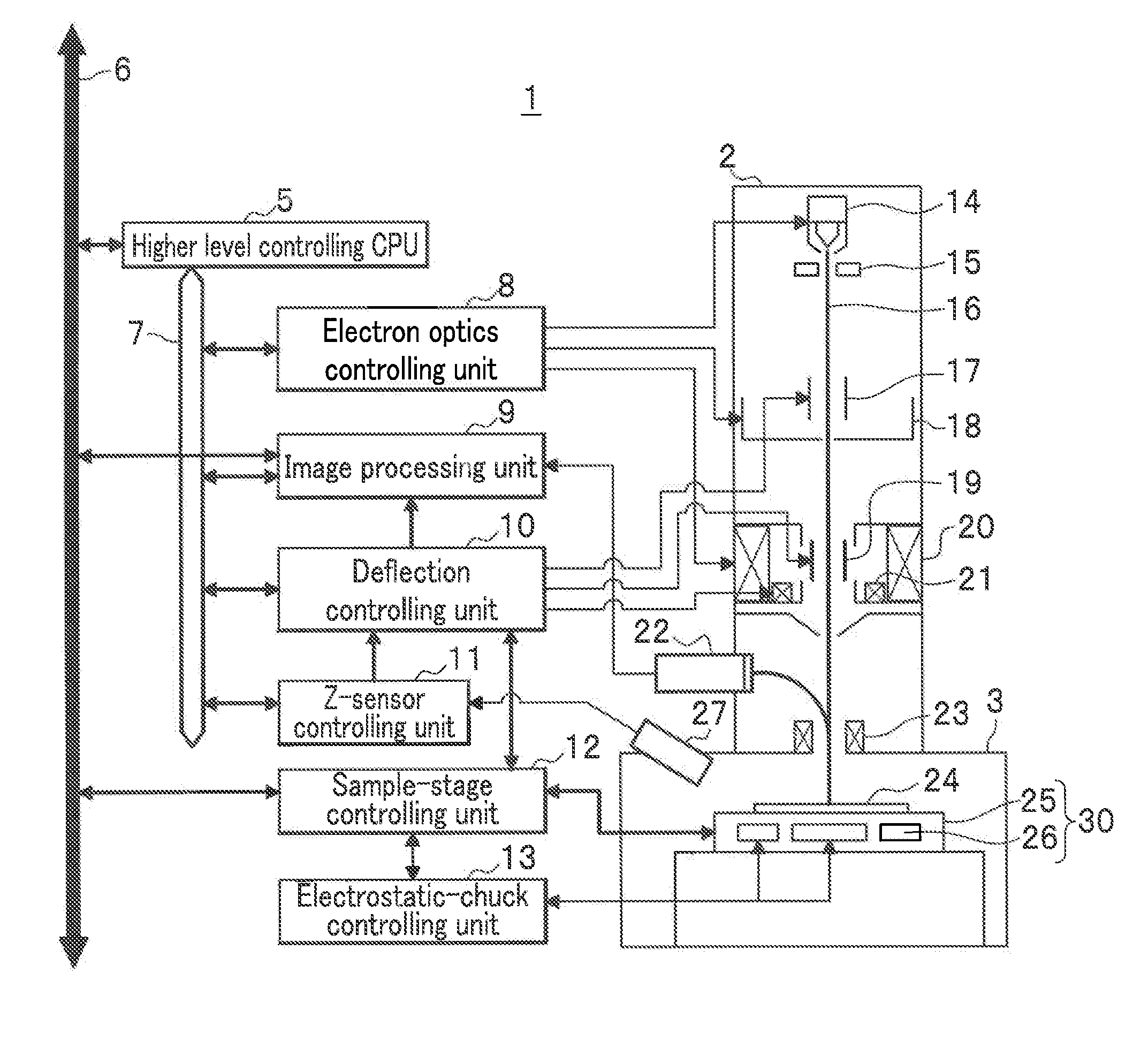
[0023]FIG. 1 is a diagram showing a structure of the charged-particle-beam apparatus 1 according to an exemplary embodiment.
[0024]As shown in FIG. 1, the charged-particle-beam apparatus 1 is provided with an electron optics column 2, a sample chamber 3, and a control system.
[0025]First, an observation operation of the charged-particle-beam apparatus 1 is described.
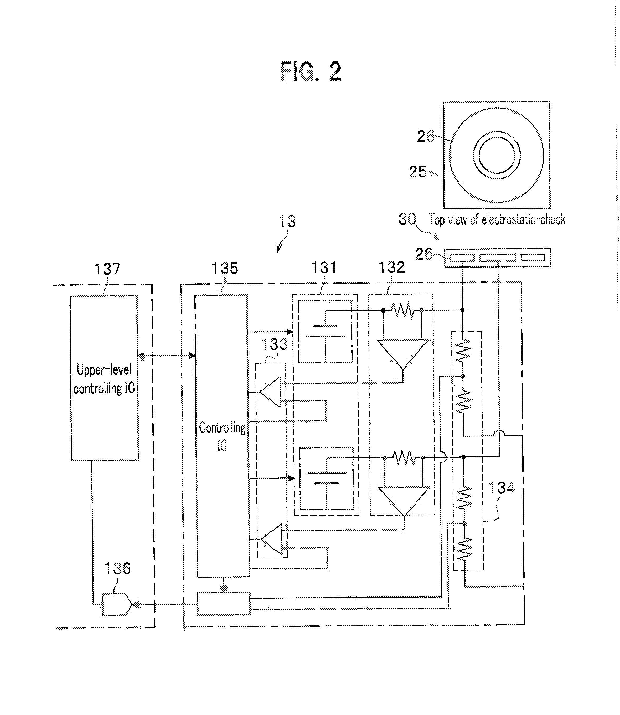
[0026]In the sample chamber 3, a wafer (sample) 24 is held on a sample stage 25 by an electrostatic chuck 30 having a chuck electrode 26. A Z-sensor 27 detects a height of the wafer 24 and outputs the height information to a Z-sensor controlling unit 11.
[0027]A primary electron beam 16 is emitted from an electron gun 14 in the electron optics c...
second embodiment
[0075]Next, a second embodiment of the present invention is described with reference to FIGS. 7A, 7B, and 8. Parts common to the first exemplary embodiment are assigned the same reference characters and the duplicate descriptions are omitted.
[0076]FIG. 7A is a diagram showing how an edge portion of the wafer 24 becomes an observed point, and FIG. 7B is a diagram showing an electric potential distribution near the edge portion of the wafer 24.
[0077]As shown in FIG. 7A, in the observing operation, the edge portion of the wafer 24 may become an observation target when the sample stage 25 moves. At this time, as shown in FIG. 713, the electric potential distribution outside of the wafer 24 falls down, which may affect the primary electron beam 16 to cause deviation in a visual field of an image of the wafer 24, and also lead to narrowing the visual field of the image.
[0078]In order to solve such a problem, when the sample stage 25 moves to the position where the edge portion of the wafe...
modified example
[0098]One exemplary embodiment according to the present invention is described above, but the present invention is not limited thereto and can be modified to the extent that the embodiment does not depart away from the subject matter of the present invention.
[0099]For example, the present invention is not limited to the charged-particle-beam apparatus described in the above embodiment, and can be widely applied for clamping a sample or the like using the electrostatic chuck.
[0100]Further, in the exemplary embodiment of the present invention, the steps of the flowchart are performed serially in time along the described order, however, the sequential processing is not essential, but the present invention also includes processing to be executed in parallel or individually.
[0101]Furthermore, appropriate combinations of the multiple components disclosed in the above embodiment can form various inventions. For example, some of all components shown in the embodiment may be deleted. Further...
PUM
 Abstract
Description
Claims
Application Information