Unlock instant, AI-driven research and patent intelligence for your innovation.
Non-volatile memory device and manufacturing method thereof
Active Publication Date: 2014-04-10
PANASONIC SEMICON SOLUTIONS CO LTD
View PDF2 Cites 22 Cited by
Summary
Abstract
Description
Claims
Application Information
AI Technical Summary
This helps you quickly interpret patents by identifying the three key elements:
Problems solved by technology
Method used
Benefits of technology
Benefits of technology
The present invention aims to reduce the possibility of thermal degradation in the manufacturing process of a non-volatile memory device. This can be achieved by implementing a specific aspect of the invention, which reduces the likelihood of such degradation. The technical effect of this invention is that it improves the manufacturing process of non-volatile memory devices by reducing the possibility of thermal degradation.
Problems solved by technology
The conventional non-volatile memory device has a problem that there is a possibility of thermal degradation in manufacturing process steps.
Method used
Image
Click on the blue label to locate the original text in one second.
Reading with bidirectional positioning of images and text.
Examples
embodiment 1
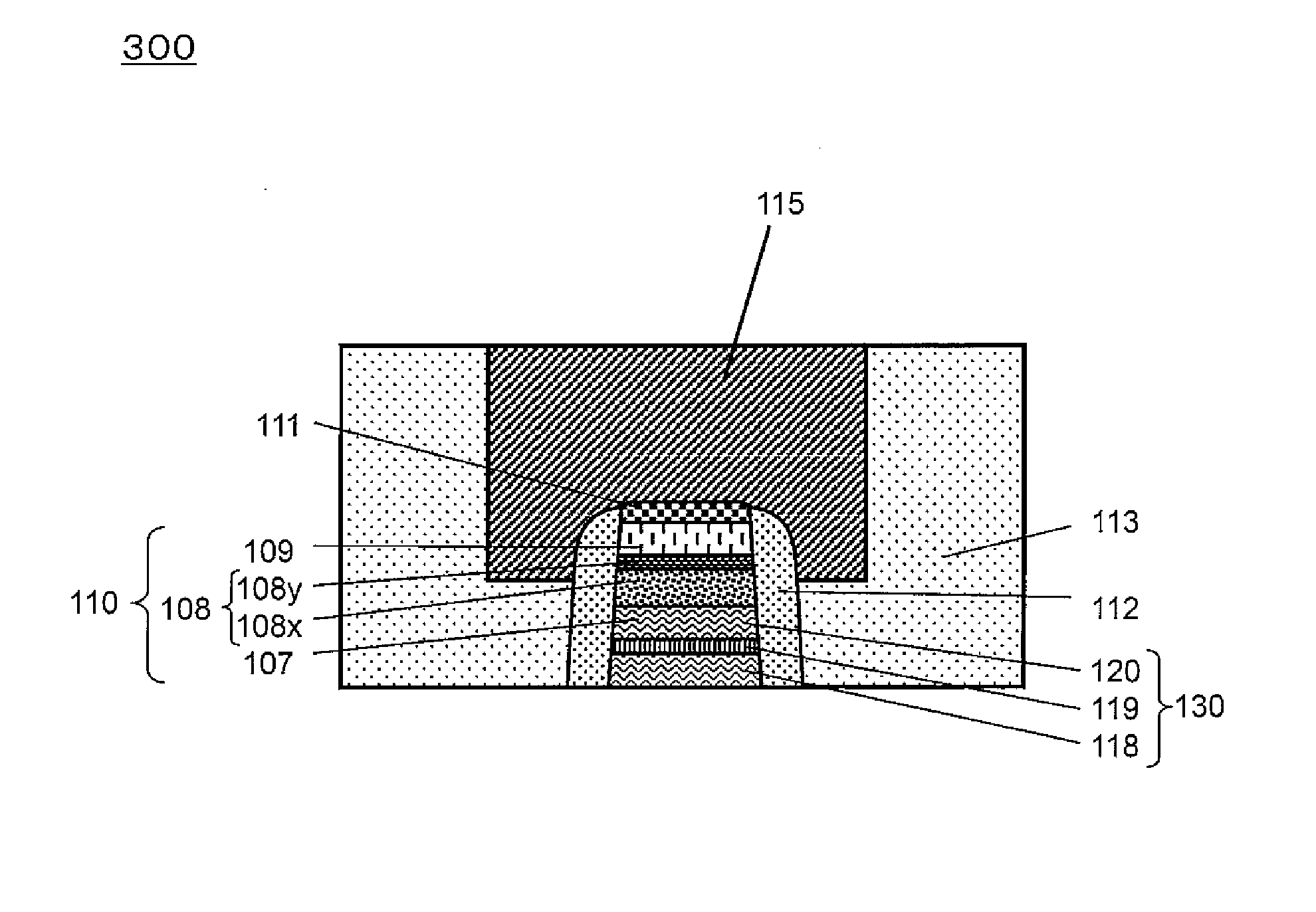
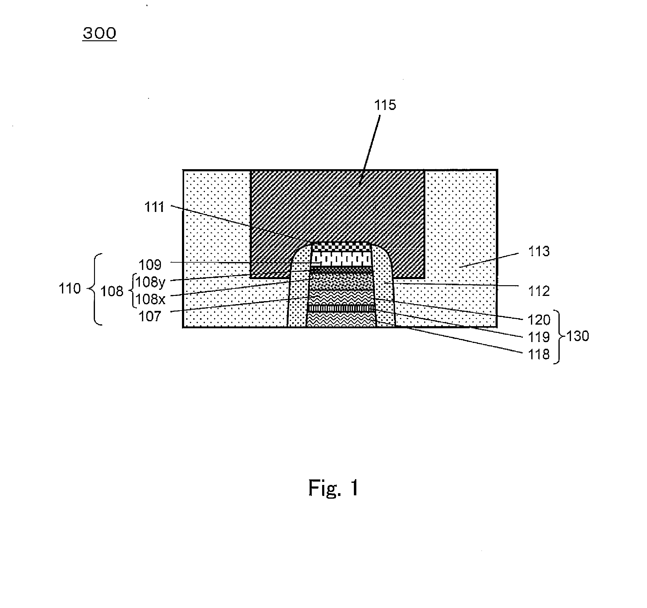
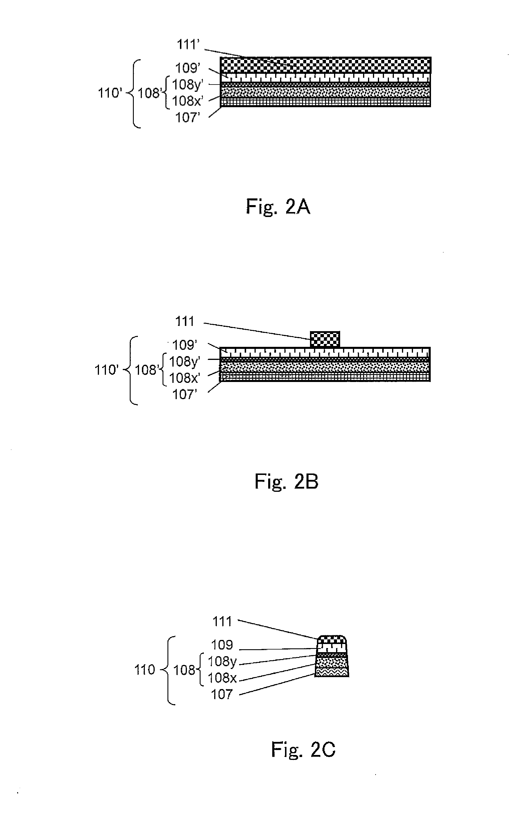
[0038]According to Embodiment 1 of the present invention, a non-volatile memory device comprises: a first electrode; a variable resistance layer formed on and above the first electrode; a second electrode formed on and above the variable resistance layer; a side wall protective layer having an insulativity and covering a side wall of the first electrode, a side wall of the variable resistance layer and a side wall of the second electrode; and an electrically-conductive layer connected to the second electrode; the non-volatile memory device including a connection layer which is provided between the second electrode and the electrically-conductive layer to connect the second electrode and the electrically-conductive layer to each other and comprises an electrically-conductive material different from a material constituting the electrically-conductive layer; wherein the side wall protective layer extends across the second electrode to a position which is above an upper end of the secon...
modified example
[0120]In the example of FIG. 1, the interlayer insulating layer 113 is formed so as cover the variable resistance element 110. In a case where the lower end of the variable resistance element 110 is in contact with the interlayer insulating layer (not shown), the substrate (not shown), etc., the interlayer insulating layer 113 may be formed so as to cover the interlayer insulating layer, the substrate, etc. The interlayer insulating layer 113 may comprise, for example, a siliconoxide having a thickness of 100 to 500 nm.
[0121]In the non-volatile memory device 100, for example, an interlayer insulating layer comprising a siliconoxide may be formed on and above a semiconductor substrate (not shown) provided with a transistor and the like.
[0122]In the non-volatile memory device 100, for example, the electrically-conductive layer may be formed inside of the interlayer insulating layer. The electrically-conductive layer may comprise, for example, a filling layer comprising copper, and a...
embodiment 2
[0180]A non-volatile memory device of Embodiment 2 is the manufacturing method of the non-volatile memory device according to any one of Embodiment 1 and modified examples of Embodiment 1 and further comprises a diode element connected to at least one of the first electrode and the second electrode.
[0181]In such a configuration, it becomes possible to surely avoid occurrence of write disturb in an adjacent variable resistance element. Thus, it becomes possible to implement a variable resistance non-volatile memory device which has a high capacity and is capable of high integration, without placing a switching element such as a transistor.
[0182]FIG. 3 is a cross-sectional view showing an exemplary schematic configuration of the non-volatile memory device according to Embodiment 2. FIG. 3 shows a portion called a memory cell array or a memory main body in a general semiconductor memory device. Hereinafter, a non-volatile memory device 300 of Embodiment 2 will be described with referen...
PUM
Abstract
A non-volatile memory device of the present invention comprises a first electrode; a variable resistance layer formed on and above the first electrode; a second electrode formed on and above the variable resistance layer; a side wall protective layer having an insulativity and covering a side wall of the first electrode, a side wall of the variable resistance layer and a side wall of the second electrode; and an electrically-conductive layer connected to the second electrode; the non-volatile memory device including a connection layer which is provided between the second electrode and the electrically-conductive layer to connect the second electrode and the electrically-conductive layer to each other, and comprises an electrically-conductive material different from a material constituting the electrically-conductive layer;wherein the side wall protective layer extends across the second electrode to a position which is above an upper end of the second electrode and below an upper end of the connection layer such that an upper end of the side wall protective layer is located above the upper end of the second electrode and below the upper end of the connection layer, when viewed from a side.
Description
CROSS-REFERENCE TO RELATED PATENT APPLICATION[0001]The application claims priority to Japanese Patent Application No. 2012-211750, filed on Sep. 26, 2012, the entire disclosure of which is incorporated herein by reference.BACKGROUND OF THE INVENTION[0002]1. Field of the Invention[0003]The present invention relates to a non-volatile memory device and a manufacturing method thereof. More particularly, the present invention relates to a variable resistance non-volatile memory device including a variable resistance element which reversibly changes its resistance value in response to an electric pulse applied thereto, and a manufacturing method thereof.[0004]2. Description of the Related Art[0005]In recent years, with progresses of digital technologies, electronic devices such as portable information devices and information home electric appliances have been developed to provide higher functionalities. With achievement of the higher functionalities of these electronic devices, further mi...
Claims
Application Information
Patent Timeline
Application Date:The date an application was filed.
Publication Date:The date a patent or application was officially published.
First Publication Date:The earliest publication date of a patent with the same application number.
Issue Date:Publication date of the patent grant document.
PCT Entry Date:The Entry date of PCT National Phase.
Estimated Expiry Date:The statutory expiry date of a patent right according to the Patent Law, and it is the longest term of protection that the patent right can achieve without the termination of the patent right due to other reasons(Term extension factor has been taken into account ).
Invalid Date:Actual expiry date is based on effective date or publication date of legal transaction data of invalid patent.

