Electroluminescent light emission device comprising an optical lattice structure and method for manufacturing same

a technology of light emission device and optical lattice structure, which is applied in the direction of thermoelectric device junction materials, semiconductor devices, electrical apparatus, etc., can solve the problems of deterioration in coupling out light, limited overall efficiency, and difficulty in integrating optical lattice structures between electrodes, so as to improve coupling out efficiency and improve system efficiency of such applications. , the effect of optimizing the coupling out ligh

Inactive Publication Date: 2014-04-17
FRAUNHOFER GESELLSCHAFT ZUR FOERDERUNG DER ANGEWANDTEN FORSCHUNG EV
View PDF12 Cites 5 Cited by
  • Summary
  • Abstract
  • Description
  • Claims
  • Application Information

AI Technical Summary

Benefits of technology

[0018]Different approaches have been examined for solving the problem of coupling out light, wherein three different OLED setup approaches are to be differentiated. On the one hand, the light may be emitted directly through a transparent top electrode to the side facing away from the substrate. Such OLEDs are called top-emitting OLEDs or TOLEDs. Here, an opaque substrate is made use of. When using transparent substrates, the light may also be emitted through the substrate itself. The OLEDs emitting through the substrate are called bottom-emitting (or substrate-emitting) OLEDs or BOLEDs. Transparent substrate contacts and opaque top contacts are made use of here. Additionally, in so-called transparent OLEDs, the light may be emitted on the substrate side and the top contact side using a transparent substrate and a transparent top contact. In BOLEDs, the coupling-out efficiency may be improved by coupling out the light bound in the substrate, for example by patterning [2] or roughening [3] the substrate. Additional approa

Problems solved by technology

The efficiency of an OLED is determined by different factors of which, in highly efficient OLEDs, in particular the efficiency of coupling out light limits the overall efficiency.
However, since, due to manufacturing factors, an ideally plane or planar surface of, for example, the intermediate layer comprising the optical lattice structure frequently cannot be manufactured when using conventional semiconductor manufacturing processes, the maximum allowable, or manufacturing-technologically achievable, unevenness of the first main surface of the intermediate layer is defined by a tolerance range in a range of less than +/−50 nm such that the organic layer may be applied onto an approximately planar surface in which the topology of the organic layer and, thus, the electrical and optical characteristics thereof are not impaired.
The present inventors have found out tha

Method used


Image

  • Electroluminescent light emission device comprising an optical lattice structure and method for manufacturing same
  • Electroluminescent light emission device comprising an optical lattice structure and method for manufacturing same
  • Electroluminescent light emission device comprising an optical lattice structure and method for manufacturing same

Examples


Embodiment Construction

[0030]Before discussing the present invention below in greater detail using drawings, it is pointed out that identical elements and structures for elements and structures having the same function or the same effect, in the different figures, are provided with same reference numerals such that the description presented in the different embodiments of the elements and structures provided with same reference numerals may be interchanged and mutually applied.

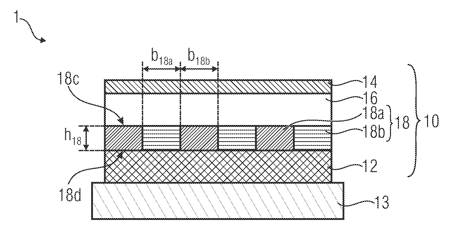
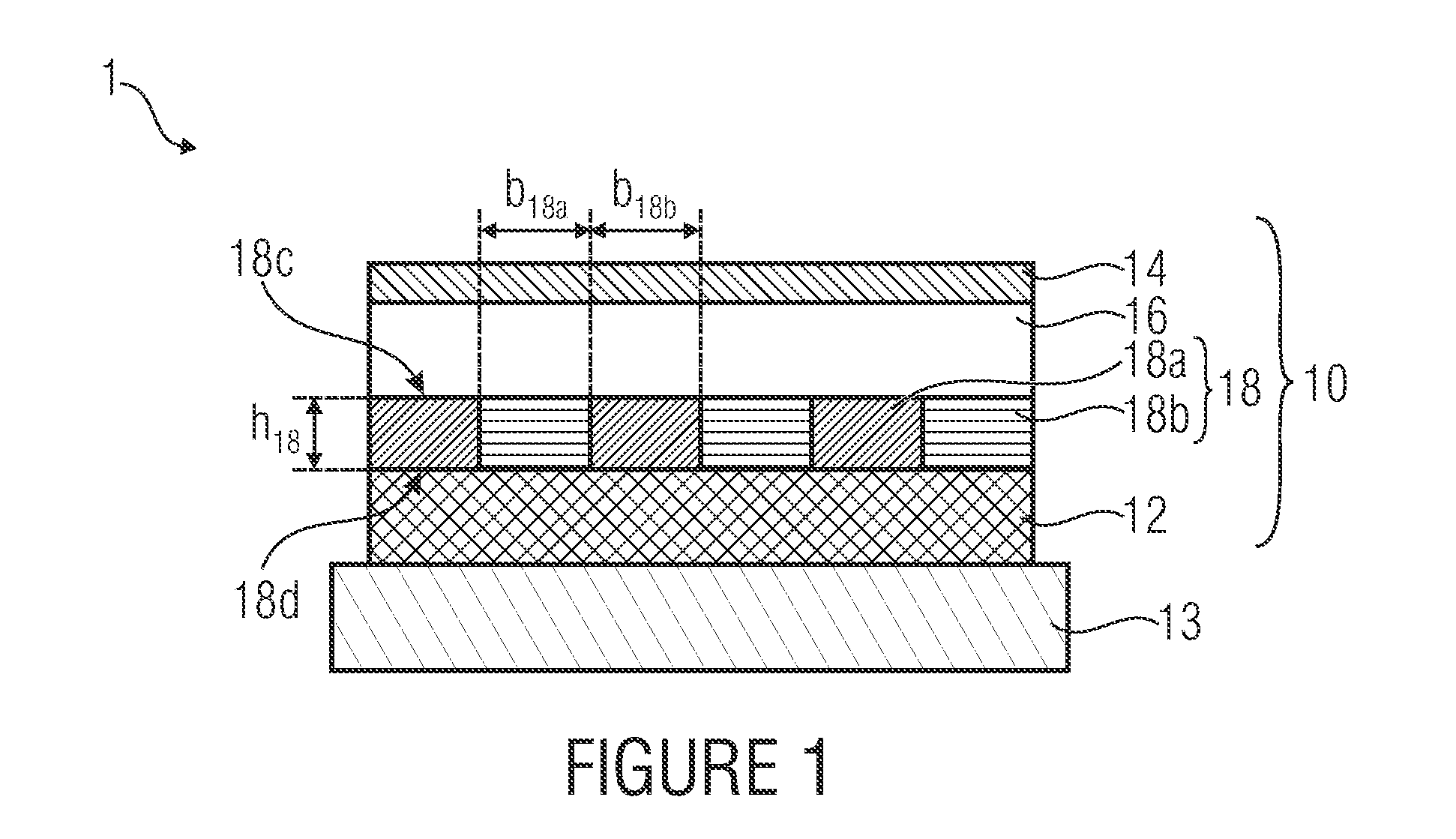
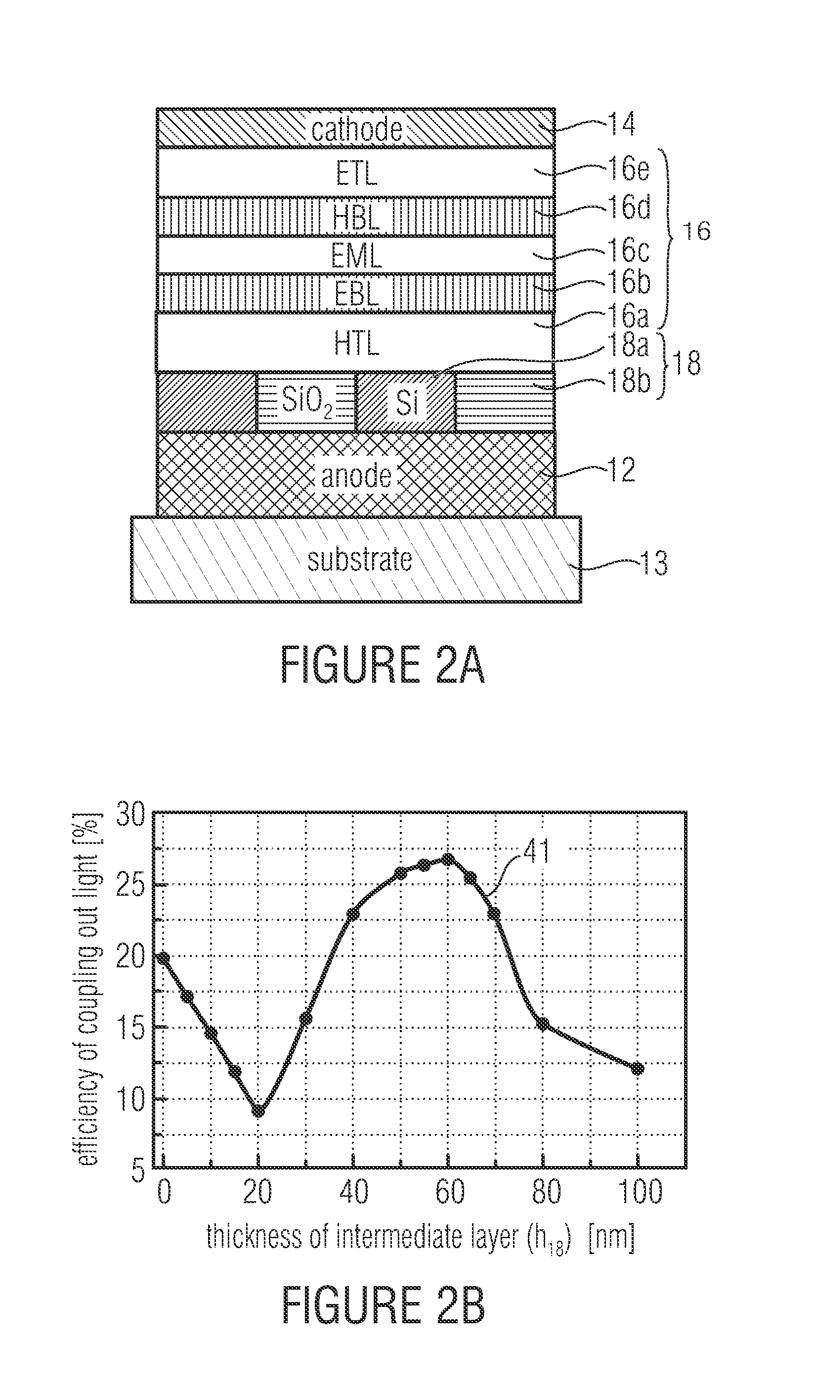
[0031]A planar electroluminescent light emission device 1 in accordance with a first embodiment of the present invention will be described making reference to FIG. 1. In particular, FIG. 1 shows a layer arrangement 10 of the light emission device 1 applied onto a substrate 13. The layer arrangement 10 comprises a first electrode layer 12 and a second electrode layer 14 which both comprise a conductive material such as, for example, aluminum. A light-emitting layer 16 made of an organic material is arranged between the two electrode ...


PUM


Abstract

A light emission device includes a substrate and a layer arrangement applied onto the substrate. The layer arrangement has a first electrode layer made of a conductive material and a second electrode layer made of a conductive material. At least one light-emitting layer made of an organic material is arranged between the first and second electrode layers. At least one intermediate layer having an optical lattice structure is provided between the light-emitting layer, a first main surface of the intermediate layer facing the light-emitting layer and the first main surface of the intermediate layer being formed to be planar within a tolerance range at least in the region of the optical lattice structure. The intermediate layer is conductive at least in regions between the first and a second main surface thereof.

Description

CROSS-REFERENCE TO RELATED APPLICATION[0001]This application is a continuation of copending International Application No. PCT / EP2012 / 062711, filed Jun. 29, 2012, which is incorporated herein by reference in its entirety, and additionally claims priority from European Application No. 11172129.6, filed Jun. 30, 2011, which is also incorporated herein by reference in its entirety.BACKGROUND OF THE INVENTION[0002]The present invention relates to an electroluminescent light emission device, such as, for example, an organic light-emitting diode or OLED, comprising an optical lattice or grating structure for improving the coupling out of light, and to a method for manufacturing same.[0003]OLEDs are increasingly employed in the field of illumination and in display technology. The potentially high efficiency, the color space achievable and the thin possible shape of OLEDs contribute particularly to this trend.[0004]The efficiency of an OLED is determined by different factors of which, in hig...

Claims


Application Information

Patent Timeline
IPC IPC(8): H01L51/52
CPCH01L51/5262H10K50/14H10K50/80H10K50/858H10K50/85
Inventor PFEIFER, RICHARDFEHSE, KARSTENVOGEL, UWELEO, KARL
Owner FRAUNHOFER GESELLSCHAFT ZUR FOERDERUNG DER ANGEWANDTEN FORSCHUNG EV
Why Eureka
Try Eureka