
Random Doping Fluctuation Resistant FinFET

a technology of metal oxides and transistors, applied in the direction of basic electric elements, electrical apparatus, semiconductor devices, etc., can solve the problems of uncertainty due to the variation in the number of dopant atoms, and the problem of nsup>1/2 /sup> comes to the for

Inactive Publication Date: 2014-04-17
SEMI SOLUTIONS +1
View PDF2 Cites 17 Cited by
  • Summary
  • Abstract
  • Description
  • Claims
  • Application Information

AI Technical Summary

Benefits of technology

The present invention is about improving the performance of metal-oxide-semiconductor field effect transistors (MOSFETs) by reducing the adverse effects of random variations in threshold voltage caused by random doping fluctuations. This is achieved by using a fin structure in the transistors, which allows for better performance and higher reliability. The invention also discusses the challenges of manufacturing MOSFETs with fins that are free of doping and the impact of uncertainty in doping atoms on the overall performance of the transistors. The invention proposes a solution to mitigate the impact of random doping variations by providing a distance of approximately 10 nm between the gate-to-channel interface and the ionized charges in the bulk. The invention is applicable to various types of three-dimensional transistors, such as FinFETs and TriGates.

Problems solved by technology

The impact of uncertainty due to variation in number of dopant atoms still continues to pose a challenge because the impact becomes more important as transistors get smaller.
Once the fins are doped, the N1 / 2 problem comes to the fore.

Method used


Image

  • Random Doping Fluctuation Resistant FinFET
  • Random Doping Fluctuation Resistant FinFET
  • Random Doping Fluctuation Resistant FinFET

Examples


exemplary embodiment 1

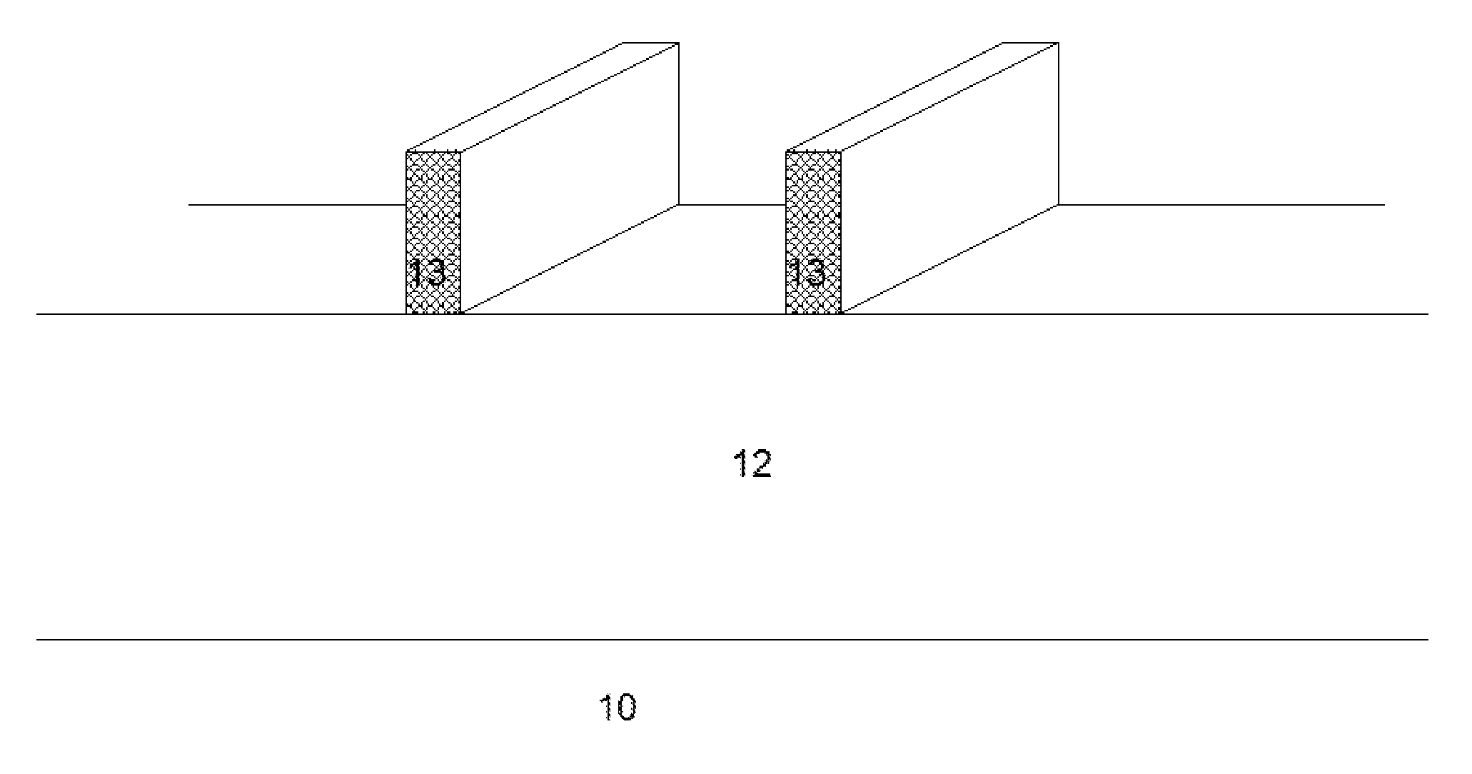
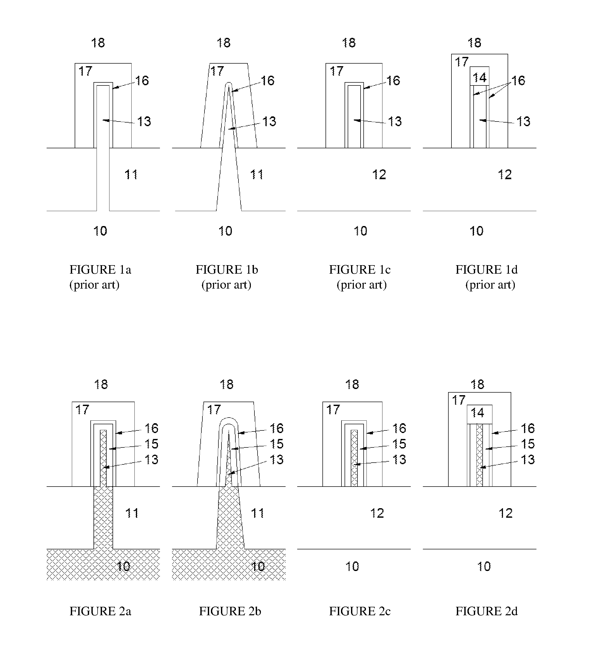
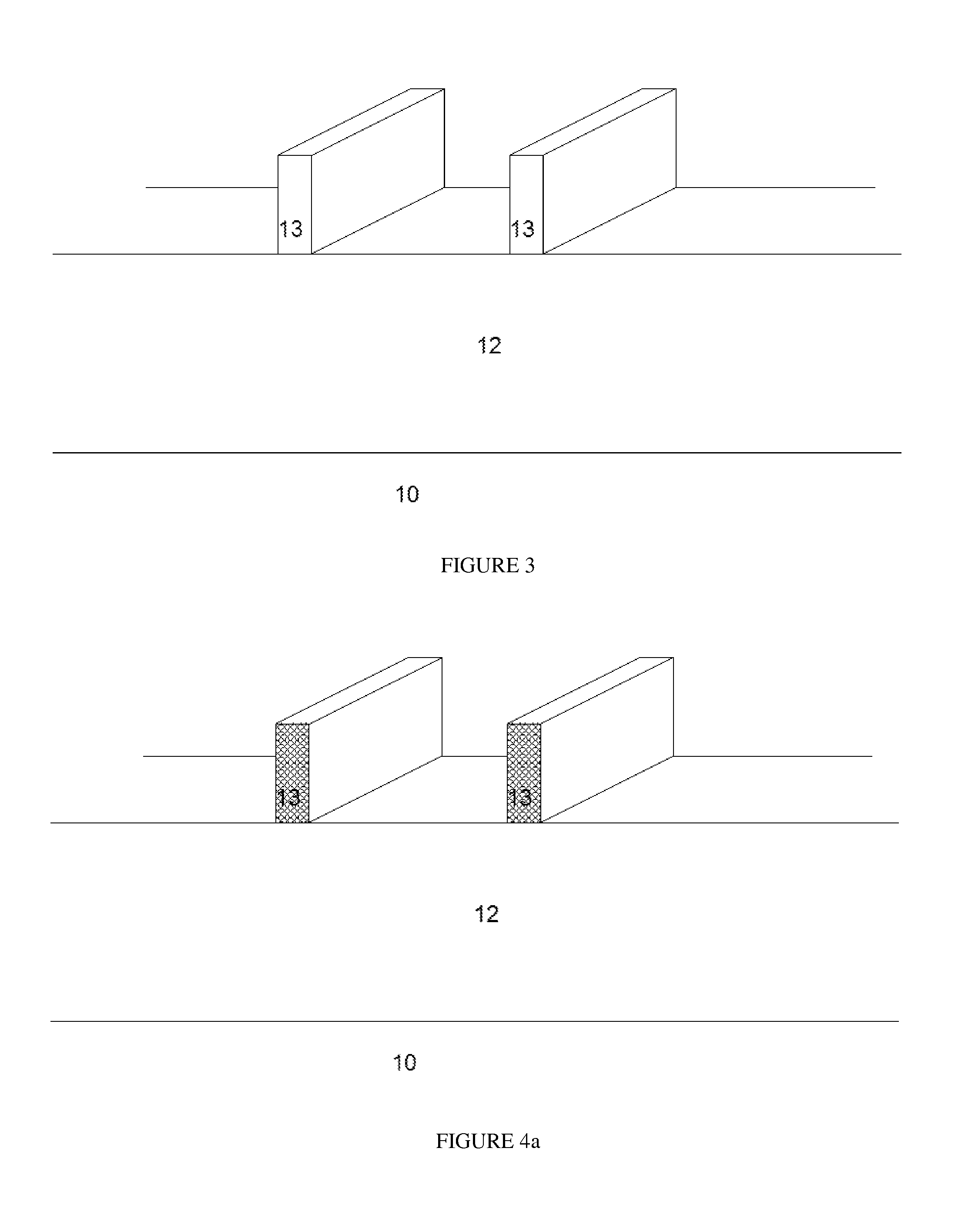
[0027]In a first exemplary and non-limiting embodiment the configuration is similar to FIG. 3, with a substrate 10 and a buried oxide 12. The fins 13 as shown in FIG. 4a are processed from the fins in FIG. 3, but rather than being lightly doped, less than 1017 / cm3 as in prior art low fluctuation transistors, they are highly doped by intention, and they will become cores for the final fins. The high doping the cores of these fins adjusts the threshold voltage of the fins to a desired high value. The fin cores are 5 nm to 15 nm thick, typically 10 nm, and they are doped with donors (for a PMOS device) or acceptors (for an NMOS device) to a density of 1018 / cm3 to 1020 / cm3. Alternatively, the highly doped fins in FIG. 4a may be formed from a highly doped layer, meaning that the heavy doping occurs before the fins are etched. For SOI fins, doping first is probably more convenient. After forming the highly doped fin cores 13, an undoped or lightly doped layer 15 of epitaxial silicon, sili...

exemplary embodiment 2

[0030]In the second exemplary and non-limiting embodiment the fins are formed from the substrate 10, as illustrated in exemplary and non-limiting FIG. 5a. The isolation oxide 11 between the fins provides a platform upon which the transistors are formed. The fins 13 in FIG. 5a are highly doped by intention to become cores for the final fins. The fin cores 13 are 5 nm to 15 nm thick, typically 10 nm, and they are doped with donors (for a PMOS device) or acceptors (for an NMOS device) to a density of 1018 / cm3 to 1020 / cm3. This doping can be done either before or after the fin cores are formed. After forming the highly doped fin cores 13, the fins are expanded by growing an undoped or lightly doped layer 15 of epitaxial silicon, silicon-germanium or other semiconductor as a sheath over the highly doped core. This is shown in exemplary and non-limiting FIG. 5b. The undoped epitaxial layer has a typical final thickness in the range of 5 nm to 15 nm, and it should be grown at a low tempera...

exemplary embodiment 3

[0032]In the third exemplary and non-limiting embodiment the initial fins 131 are also formed from the substrate 10, as illustrated in FIG. 6a. Between the initial fins 131 the isolation oxide 11 provides a platform upon which the transistors are formed. The initial fins 131 in FIG. 6a are highly doped by intention, but they are wider than the fin cores 13 in Embodiment 2 as they are subject to additional processing. The initial fins 131 are 15 nm to 50 nm thick, typically 30 nm, and they are doped with donors (for a PMOS device) or acceptors (for an NMOS device) to a density of 1018 / cm3 to 1020 / cm3. The doping in the fins is determined by the desired threshold voltage. This doping can be done either before or after the initial fins are formed. The next step, shown in exemplary and non-limiting FIG. 6b, is an etching step that removes a portion of the initial fins 131 to leave fin cores 13, which are typically 5 nm to 15 nm wide. After the etching step leaves the highly doped fin co...


PUM


Abstract

An improved fin field-effect transistor (FinFET) is built on a compound fin, which has a doped core and lightly doped epitaxial channel region between that core and the gate dielectric. The improved structure reduces FinFET random doping fluctuations when doping is used to control threshold voltage. Further, the transistor design affords better source and drain conductance when compared to prior art FinFETs. Three representative embodiments of the key structure are described in detail.

Description

CROSS-REFERENCE TO RELATED APPLICATIONS[0001]This application claims the benefit of U.S. Provisional Patent Application No. 61 / 713,632 filed Oct. 15, 2012.BACKGROUND OF THE INVENTION[0002]1. Field of the Invention[0003]The present invention generally relates to the manufacturing of metal-oxide-semiconductor field effect transistors (MOSFETs), and more particularly to FinFETs and other transistors based on an active region perpendicular to the plane of the silicon wafer. Even more specifically, this invention deals with those instances where random variations of the threshold voltages of such transistors adversely affect integrated circuit performance.[0004]2. Prior Art[0005]Transistors built on a silicon fin were demonstrated as early as 1991 (Hisamoto, D., et al., “Impact of the vertical SOI ‘DELTA’ structure on planar device technology,”Electron Devices, IEEE Transactions on, vol. 38, no. 6, pp. 1419-1424, June 1991) with the goal of achieving better transconductance and superior ...

Claims


Application Information

Patent Timeline
IPC IPC(8): H01L29/78H01L29/66
CPCH01L29/66795H01L29/785H01L29/7853
Inventor KAPOOR, ASHOK K.STRAIN, ROBERT J.
Owner SEMI SOLUTIONS
Learn More