Low Cost High Density Nonvolatile Memory Array Device Employing Thin Film Transistors and Back to Back Schottky Diodes

Inactive Publication Date: 2014-04-17
TACHO HLDG LLC
View PDF5 Cites 38 Cited by
  • Summary
  • Abstract
  • Description
  • Claims
  • Application Information

AI Technical Summary

Benefits of technology

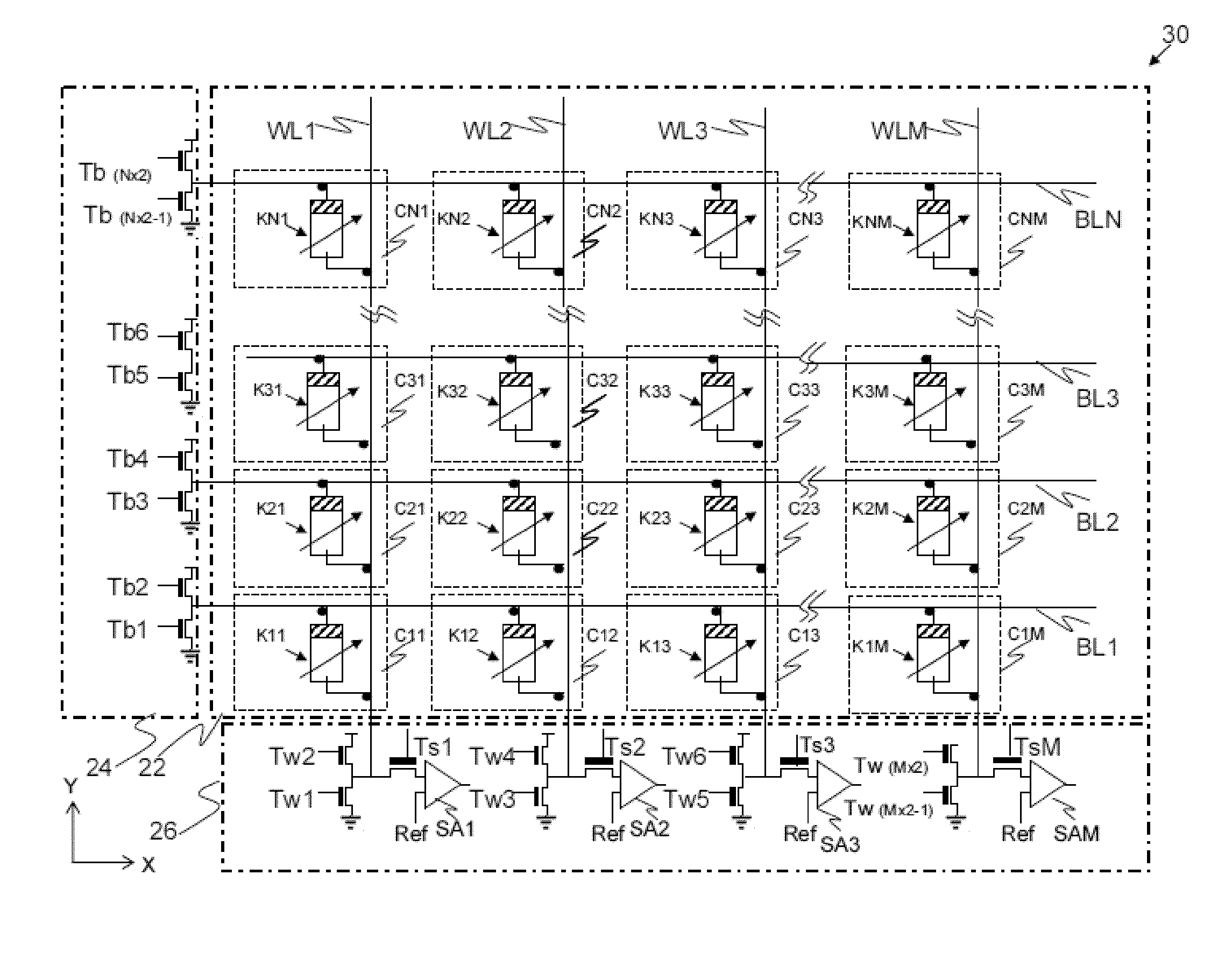
[0086]A key advantage of the present invention is that the technology nodes for fabrication of the memory array (MTJ layer) and TFT array (TFT layer) are decoupled. In other words, depending on the desired functionality of the TFT layer, one may use the same technology node (for example, 45 nm) used to fabricate the MTJ layer to fabricate the TFTs, or preferably, in order to reduce cost and given the fact there is a significantly smaller number of TFTs needed ((2×N)+(3×M)) compared to the number of memory elements (M×N), a larger technology node (for example, 65 nm, 90 nm, 130 nm or larger yet) may be employed during the fabrication of the TFTs. In addition, there is no need to place the TFTs along the perimeter of the memory array as disclosed in US 2012/0281465; rather, the TFTs are fabricated directly over or under the memory array to be addressed. Interconnection of the TFTs to their respective conductive lines is done vertically with no need for complex lateral interconnects. TFTs do not require the front end process equipment required in MOS foundries; hence, the cost of TFTs are substantially lower than MOS based transistors. Eliminating the need for MOS based transistors allows for use of low cost glass substrates.
[0087]The selection thin-film transistors can be disposed below or above magnetic tunnel junctions (or junctions). A gate width of the selection transistor can be significantly larger that a width (or a diameter) of the magnetic tunnel junction. A memory cell can have one transistor—several magnetic tunnel junctions (1T-nMTJ) arrangement. The magnetic tunnel junctions are jointly electrically connected to a selection transistor at their first ends and independently electrically coupled to an appropriate conductive line (bit or word line) at their second ends. A data can be recorded to magnetic tunnel junction by a spin-induced switching mechanism or by a hybrid switching mechanism including simultaneous effect of the spin-polarized current and a bias magnetic field applied to the magnetic tunnel junction.
[0088]FIG. 10 is a top view illustration showing the interconnects of conductive lines (either bit line

Problems solved by technology

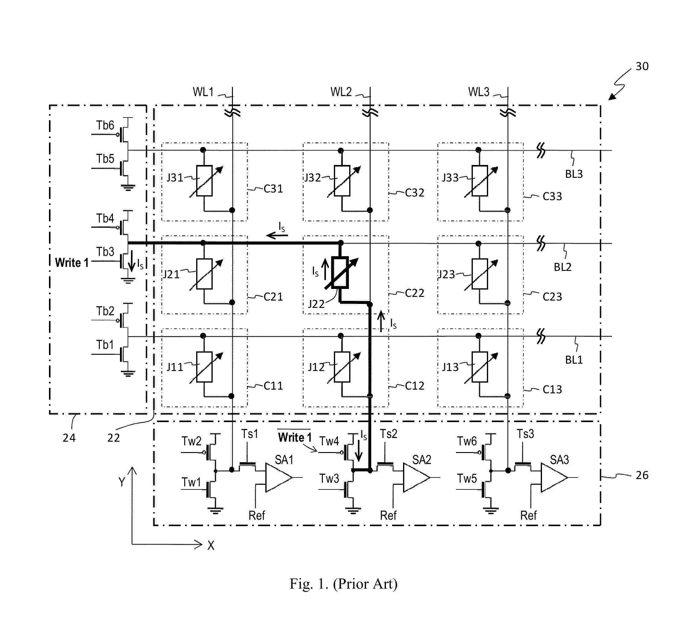
The circuit described by US 2012/0281465 presents a challenge to controlling the addressing of the memory array for writing, reading or erasing due to the fact alternative current paths are possible than those described in the disclosure.
The use of MOS

Method used


Image

  • Low Cost High Density Nonvolatile Memory Array Device Employing Thin Film Transistors and Back to Back Schottky Diodes
  • Low Cost High Density Nonvolatile Memory Array Device Employing Thin Film Transistors and Back to Back Schottky Diodes
  • Low Cost High Density Nonvolatile Memory Array Device Employing Thin Film Transistors and Back to Back Schottky Diodes

Examples


first embodiment

[0110]FIG. 7 is a cross section view of a three-dimensional memory array made in accordance with a first embodiment of the present invention. Memory arrays (63) are cross-point MRAM arrays made according to FIG. 6 whereby a BBSD is incorporated into each memory element. A silicon wafer substrate (60) is provided with CMOS circuitry (61) fabricated on the substrate. Such circuitry is fabricated at a technology node (Fc) which may be the same size as the technology node for the MTJ layers (Fm) or smaller or larger, depending on the nature of the CMOS circuitry. For example, a microprocessor or high end FPGA may be fabricated at a smaller technology node Fc compared to the embedded memory array (Fm) which resides above the circuitry. This embedded memory is lower cost than a separate chip and provides for higher speeds as no off chip delays a required. Lower power consumption is also realized due to the reduced circuitry. On the other hand, a stand alone memory device may have a larger...

second embodiment

[0111]FIG. 8 is a cross section view of a three-dimensional memory array made in accordance with a second embodiment of the present invention. Memory arrays (63) are cross-point MRAM arrays made according to FIG. 6 whereby a BBSD is incorporated into each memory element. A low cost glass substrate (70) is provided with the first thin film transistor layer (TFT-L1) circuitry fabricated on the substrate. Such circuitry is fabricated at a technology node (Ft) which may be the same size as the technology node for the MTJ layers (Fm) but preferably for cost savings may be larger than Fm. Such circuitry may include the bandgap and decoder logic for the memory arrays (63), as well as selection transistors for the first memory array (MTJ-L1). Additional circuitry for the memory arrays (MTJ-L1-MTJ-Ln) is provided in various additional layers (64) of thin film transistors (TFT-L2-TFT-Ln+1) disposed between the memory arrays. The TFT circuitry is fabricated at a technology node (Ft) substantia...

third embodiment

[0112]FIG. 9 is a cross section view of a three-dimensional memory array made in accordance with a third embodiment of the present invention. Memory arrays (63) are cross-point MRAM arrays made according to FIG. 6 whereby a BBSD is incorporated into each memory element. A low cost glass substrate (70) is provided with the first thin film transistor layer (TFT-L1) circuitry fabricated on the substrate. Such circuitry is fabricated at a technology node (Ft) which may be the same size as the technology node for the MTJ layers (Fm) but preferably for cost savings may be larger than Fm. Such circuitry may include the bandgap and decoder logic for the memory arrays (63), as well as selection transistors for the first memory array (MTJ-L1). Additional circuitry for the memory arrays (MTJ-L1-MTJ-Ln) is provided in various additional layers (64) of thin film transistors (TFT-L2-TFT-L(n / 2+1) disposed between every two memory arrays. The TFT circuitry is fabricated at a technology node (Ft) su...


PUM


Abstract

An improved crosspoint memory array device comprising a plurality of memory cells, each memory cell being disposed at an intersection region of bit and word conductive lines, electrically coupled to one of the first conductive lines at a first terminal and to one of the second conductive lines at a second terminal, and comprising a controllable electrical resistance, wherein a back to back Schottky diode is located between each memory cell and one of the said conductive lines, and wherein each conductive line is electrically coupled to at least two thin film transistors (TFTs). The device is substantially produced in BEOL facilities without need of front end semiconductor production facilities, yet can be made with ultra high density and low cost.

Description

CROSS-REFERENCE TO RELATED APPLICATIONS[0001]This application claims priority to Provisional Patent Application No. 61 / 699,211 having a filing date of Sep. 10, 2012 and to Provisional Patent Application No. 61 / 702,485 having a subsequent filing date.FEDERALLY SPONSORED RESEARCH: None[0002]SEQUENCE LISTING: None.PRIOR ART REFERENCES[0003]U.S. Patent Application publication 2012 / 0281465, Nov. 8, 2012—Agan et. al.[0004]U.S. Patent Application publication 2012 / 0257449, Oct. 11, 2012—Agan et. al.[0005]U.S. Pat. No. 6,750,540, Jun. 15, 2004—Kim[0006]U.S. Pat. No. 5,640,343, Jun. 17, 1997—Gallagher et. al.[0007]U.S. Pat. No. 7, 224,601, May 29, 2007—Panchula[0008]U.S. Pat. No. 7,529,121, May 5, 2009—Kitagawa et. al.[0009]U.S. Pat. No. 6,838,721, Jan. 4, 2005—Garni et. al.[0010]U.S. Pat. No. 7,668,005, Feb. 23, 2010—Ueda[0011]U.S. Patent Application publication 2010 / 0213458, Aug. 26, 2010—Prall[0012]U.S. Pat. No. 8,411,494, Apr. 2, 2013—Shukh[0013]U.S. Pat. No. 8,227,788, Jul. 24, 2012—Mika...

Claims


Application Information

Patent Timeline
IPC IPC(8): H01L27/22
CPCH01L27/224G11C13/0007G11C2213/72G11C11/161G11C11/165G11C2213/71H10B61/10
Inventor LUPINO, JAMES JOHNAGAN, TOMMY ALLEN
Owner TACHO HLDG LLC
Why Eureka
Try Eureka