Structured light 3D scanner with refractive non-absorbing pattern forming element

a structured light and pattern forming technology, applied in the field of structured light 3d scanners, can solve the problems of increasing the size, energy consumption and price of the system, reducing the achieved accuracy, and affecting the accuracy of the time of flight approach, so as to achieve low cost, compact size and weight, and low power consumption.

Inactive Publication Date: 2014-04-24
BLAYVAS ILYA
View PDF6 Cites 37 Cited by
  • Summary
  • Abstract
  • Description
  • Claims
  • Application Information

AI Technical Summary

Benefits of technology

[0018]The present invention has multiple advantages over state of the art scanners. One embodiment of present invention has similar architecture to that described in Ser. No. 11/750,029, which is incorporated here by reference, and therefore heritages the same advantages over the prior art: compact size and weight, low power consumption, low cost, high accuracy etc.
[0019]Furthermore, Ser. No. 11/750,029 teaches us a method and apparatus of a pattern projector using a light-absorbing mask, with sine-modulated transparency. The present invention however demonstrates how same, similar or differ...

Problems solved by technology

The time of flight approach suffers from several limitations.
Providing high energy concentration into the ultra-short pulses, using ultra-fast light gates, and accurate measurements of the flight time are physically challenging tasks, requiring expensive and bulky electronics, increasing the size, energy consumption and price of the systems, and decreasing the achieved accura...

Method used


Image

  • Structured light 3D scanner with refractive non-absorbing pattern forming element
  • Structured light 3D scanner with refractive non-absorbing pattern forming element
  • Structured light 3D scanner with refractive non-absorbing pattern forming element

Examples


Embodiment Construction

[0036]Many aspects of the present disclosure can be better understood with reference to the following drawings. The components in the drawings are not necessarily to scale, emphasis instead being placed upon clearly illustrating the principles of the present disclosure. In the drawings, like reference numerals designate corresponding parts throughout the several views.

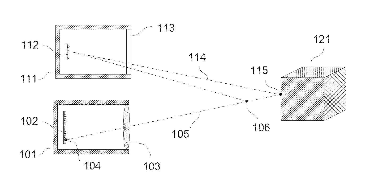
[0037]FIG. 1 illustrates the operation principles of structured light 3D scanner. It schematically shows an imaging camera 101, pattern projector 111 and an object 121. A pixel 104 of a camera image sensor 102 images the object point 115. However, the depth information is lost in the camera, and the same pixel 104 can correspond to any point along the ray 105, for example to a point 106. The pattern projector allows solving this ambiguity, by providing auxiliary illumination in the forms of specially designed patterns. From one or more images acquired under patterned illumination from pattern projector 111, with the in...


PUM


Abstract

A structured light 3D scanner consisting of a pattern projector; a digital imaging camera; and a controlling and processing circuitry is disclosed. Several novel variants of pattern projector are claimed. One embodiment comprises one or more transparent refractive pattern forming element, and two or more independently switchable light sources. Another embodiment comprises an array of light emitting diodes (LEDs), grown on the same semiconductor substrate, and an optical lens projecting the image formed by the said diode array.
Sequential acquisition of video frames with synchronous switching between the light sources in the pattern projector produces a sequence of images obtained under different illumination patterns. Processing these images produces a sequence of 3D scans of the scene.

Description

CROSS REFERENCE TO RELATED APPLICATIONS[0001]11 / 750,029November 2008Blayvas356 / 6037,224,384May 2007Iddan et al.348 / 207.997,057,654June 2006Roddy et al.348 / 277; 348 / 2796,788,210September 2004Huang et al.340 / 612; 382 / 154;382 / 2866,781,676August 2004Wallace et al.356 / 4.03; 250 / 221;250 / 559.29;6,885,464April 2005Pfeiffer et al.356 / 602; 356 / 603;433 / 296,057,909May 2000Yahav et al.356 / 5.04;313 / 103CM;313 / 105CM;5,965,875October 1999Merrill250 / 226; 250 / 208.1;250 / 214.1;4,802,759February 1989Matsumoto et al.356 / 603; 356 / 3.03;702 / 1674,687,326August 1987Corby Jr.356 / 5.01; 2, 5.04,141.4, 141.5,4,611,292September 1986Ninomiya et al.702 / 153; 152348 / 94; 382 / 153;STATEMENT REGARDING FEDERALLY SPONSORED RESEARCH OR DEVELOPMENT[0002]Not Applicable.REFERENCE TO SEQUENCE LISTING[0003]Nor Applicable.BACKGROUND OF THE INVENTION[0004]This invention belongs to the field of structured light 3D scanners. 3D scanners acquire a three dimensional shape of the object and are used in multiple applications, such as: Gam...

Claims


Application Information

Patent Timeline
IPC IPC(8): F21V9/00H04N13/02H04N13/20
CPCH04N13/02F21V9/00G01B11/2513G01B11/2531H04N13/20
Inventor BLAYVAS, ILYA
Owner BLAYVAS ILYA
Why Eureka
Try Eureka