
High efficiency CZTSe by a two-step approach

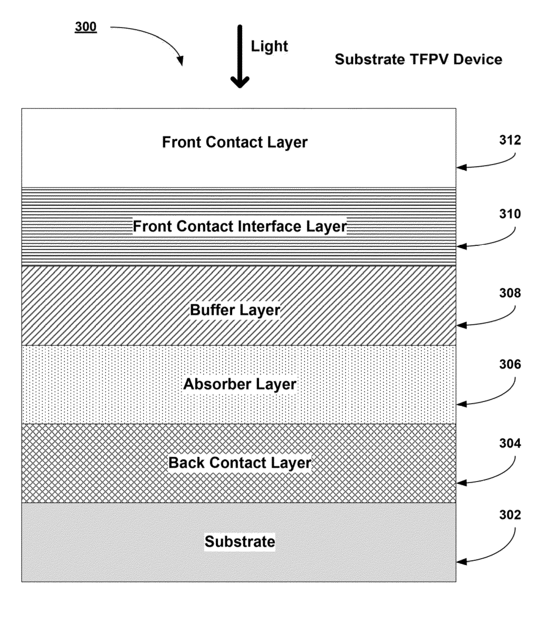
a technology of thin film and high efficiency, applied in the direction of semiconductor/solid-state device manufacturing, semiconductor devices, electrical equipment, etc., can solve the problems of increasing manufacturing costs, increasing costs, and reducing manufacturing costs of crystalline silicon solar cells,

Inactive Publication Date: 2014-04-24
INTERMOLECULAR
View PDF3 Cites 27 Cited by
  • Summary
  • Abstract
  • Description
  • Claims
  • Application Information

AI Technical Summary

Benefits of technology

This patent describes a method for making a special absorber layer in a device called a TFPV. The layer is made by sputtering a film of a specific mixture of materials, which is then converted to a layer through a process called selenization. The resulting layer has a graded bandgap, which helps to improve the device's performance. The technical effect of this method is to provide a more efficient and effective absorber layer for TFPV devices.

Problems solved by technology

The use of a thick substrate also means that the crystalline silicon solar cells must use high quality material to provide long carrier lifetimes. Therefore, crystalline silicon solar cell technologies lead to increased costs.
TFPV devices can be fabricated at the cell level or the panel level, thus further decreasing the manufacturing costs.
A number of Earth abundant, direct-bandgap semiconductor materials now seem to show evidence of the potential for both high efficiency and low cost in Very Large Scale (VLS) production (e.g. greater than 100 gigawatt (GW)), yet their development and characterization remains difficult because of the complexity of the materials systems involved.
However, the supply of In, Ga and Te may impact annual production of CIGS and CdTe solar panels.
Moreover, price increases and supply constraints in Ga and In could result from the aggregate demand for these materials used in flat panel displays (FPD) and light-emitting diodes (LED) along with CIGS TFPV.
Also, there are concerns about the toxicity of Cd throughout the lifecycle of the CdTe TFPV solar modules.
The development of TFPV devices exploiting Earth abundant materials represents a daunting challenge in terms of the time-to-commercialization.
Traditional R&D methods are ill-equipped to address such complexity, and the traditionally slow pace of R&D could limit any new material from reaching industrial relevance when having to compete with the incrementally improving performance of already established TFPV fabrication lines, and continuously decreasing panel prices for more traditional cSi PV technologies.
Due to the complexity of the material, cell structure, and manufacturing process, both the fundamental scientific understanding and large scale manufacturability are yet to be realized for TFPV devices.

Method used


Image

  • High efficiency CZTSe by a two-step approach
  • High efficiency CZTSe by a two-step approach
  • High efficiency CZTSe by a two-step approach

Examples


Embodiment Construction

[0035]A detailed description of one or more embodiments is provided below along with accompanying figures. The detailed description is provided in connection with such embodiments, but is not limited to any particular example. The scope is limited only by the claims and numerous alternatives, modifications, and equivalents are encompassed. Numerous specific details are set forth in the following description in order to provide a thorough understanding. These details are provided for the purpose of example and the described techniques may be practiced according to the claims without some or all of these specific details. For the purpose of clarity, technical material that is known in the technical fields related to the embodiments has not been described in detail to avoid unnecessarily obscuring the description.

[0036]It must be noted that as used herein and in the claims, the singular forms “a,”“an,” and “the” include plural referents unless the context clearly dictates otherwise. Th...


PUM

PropertyMeasurementUnit
pressureaaaaaaaaaa
pressureaaaaaaaaaa
pressureaaaaaaaaaa

Abstract

Methods of forming CZTS absorber layers in a TFPV device with a graded bandgap with or without a graded concentration are provided. In general, a Cu—Zn—Sn—(S, Se) precursor film is formed by sputtering. The Cu—Zn—Sn—(S, Se) precursor film can be formed as a single layer or as a multilayer stack. The composition may be uniform or graded throughout the thickness of the film. In some embodiments, the sputtering is performed in a reactive atmosphere including a chalcogen source (e.g. H2S, H2Se, etc.). The films, in conjunction with a subsequent selenization or anneal process, are converted to an absorber layer.

Description

CROSS-REFERENCE TO RELATED APPLICATIONS[0001]This application is a Continuation-in-Part of U.S. patent application Ser. No. 13 / 595,888 filed on Aug. 27, 2012, which further claims priority to U.S. Provisional Patent Application Ser. No. 61 / 578,691 filed on Dec. 21, 2011, each of which are herein incorporated by reference for all purposes.FIELD OF THE DISCLOSURE[0002]This disclosure relates to thin film photovoltaic devices, and more particularly, to an absorber layer for a thin film photovoltaic device that has a graded bandgap, and methods of forming the same. More specifically, methods of developing absorbers for copper zinc tin (sulfide) selenide (CZT(S)Se, or CZTS) solar cells are discussed.BACKGROUND OF THE DISCLOSURE[0003]Solar cells are photovoltaic (PV) devices that convert light into electrical energy. Solar cells have been developed as clean, renewable energy sources to meet growing demand. Solar cells have been implemented in a wide number of commercial markets including ...

Claims


Application Information

Patent Timeline
Patent Type & Authority Applications(United States)
IPC IPC(8): H01L31/18
CPCH01L21/02568H01L21/02573H01L21/02614H01L31/065H01L21/02554H01L31/0322Y02E10/541H01L31/0326H01L21/02551H01L21/02557H01L21/0256H01L31/0749
Inventor VAN DUREN, JEROENCARDOZO, BENLIANG, HAIFAN
Owner INTERMOLECULAR
Learn More