Sample Inspection System Detector

a detection system and sample technology, applied in the direction of material analysis, instruments, radiation control devices, etc., can solve the problems of inspection systems, damage to the wafer surface, limited sensitivity of typical detector arrays, etc., to optimize the dynamic range of the overall detector system, increase the dynamic range of the inspection system, and improve the effect of the overall detector system

Active Publication Date: 2014-05-01
KLA TENCOR TECH CORP
View PDF1 Cites 18 Cited by
  • Summary
  • Abstract
  • Description
  • Claims
  • Application Information

AI Technical Summary

Benefits of technology

[0011]In one aspect, the dynamic range of the inspection system is increased by directing a portion of the light collected from each pixel of the wafer inspection area toward an array of avalanche photodiodes operating in Geiger mode and directing another portion of the light collected from each pixel of the wafer inspection area toward another array of photodetectors (e.g., an array of avalanche photodiodes operating in linear mode, PIN photodiodes, PMTs, CCD

Problems solved by technology

Typical detector arrays are limited in their sensitivity due to significant detector noise.
Often, this results in inspection systems that operate in a detector noise limited regime, rather than a photon limited, or surface limited regime.
However, in high-power, laser-based inspection systems, increasing the power density of the incident laser beam may cause damage to the wafer surface.
In addition, increasing the illumination power, particularly at short wavelengths, increases cost and may introduce reliability risks.
PMTs, for example, are typically bulky, and require high dr

Method used


Image

  • Sample Inspection System Detector
  • Sample Inspection System Detector
  • Sample Inspection System Detector

Examples


Embodiment Construction

[0036]Reference will now be made in detail to background examples and some embodiments of the invention, examples of which are illustrated in the accompanying drawings.

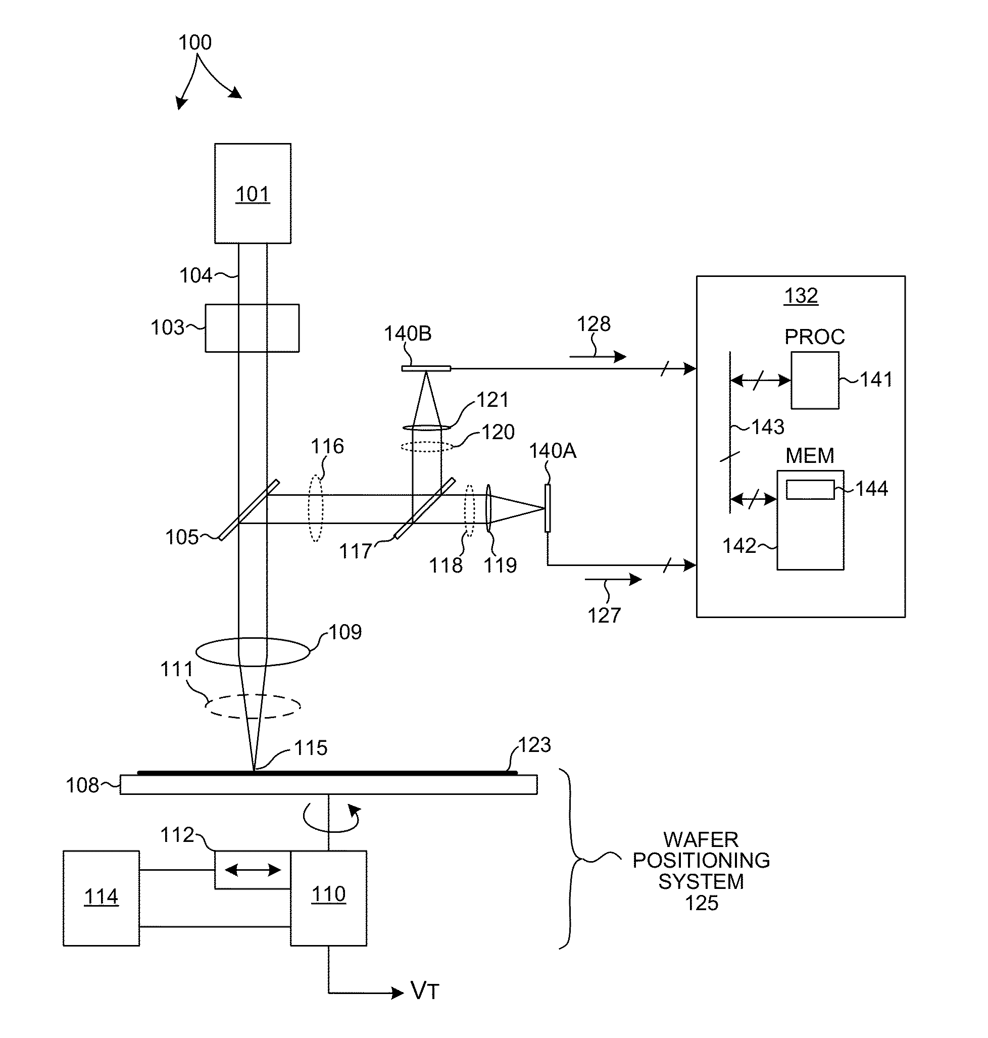
[0037]FIG. 1 is a simplified schematic view of one embodiment of a surface scanning inspection system 100 that may be used to perform the inspection methods described herein. For simplification, some optical components of the system have been omitted. By way of example, folding mirrors, polarizers, beam forming optics, additional light sources, additional collectors, and additional detectors may also be included. All such variations are within the scope of the invention described herein. The inspection system described herein may be used for inspecting patterned, as well as unpatterned wafers.

[0038]As illustrated in FIG. 1, a wafer 123 is illuminated by a normal incidence beam 111 generated by one or more illumination sources 101. Alternatively, the illumination subsystem may be configured to direct the beam of light ...


PUM


Abstract

Methods and systems for enhancing the dynamic range of a high sensitivity inspection system are presented. The dynamic range of a high sensitivity inspection system is increased by directing a portion of the light collected from each pixel of the wafer inspection area toward an array of avalanche photodiodes (APDs) operating in Geiger mode and directing another portion of the light collected from each pixel of the wafer inspection area toward another array of photodetectors having a larger range. The array of APDs operating in Geiger mode is useful for inspection of surfaces that generate extremely low photon counts, while other photodetectors are useful for inspection of larger defects that generate larger numbers of scattered photons. In some embodiments, the detected optical field is split between two different detectors. In some other embodiments, a single detector includes both APDs operating in Geiger mode and other photodetectors having a larger range.

Description

CROSS REFERENCE TO RELATED APPLICATION[0001]The present application for patent claims priority under 35 U.S.C. §119 from U.S. provisional patent application Ser. No. 61 / 719,048, entitled “Sample Inspection System,” filed Oct. 26, 2012, the subject matter of which is incorporated herein by reference.TECHNICAL FIELD[0002]The described embodiments relate to systems for surface inspection, and more particularly to semiconductor wafer inspection modalities.BACKGROUND INFORMATION[0003]Semiconductor devices such as logic and memory devices are typically fabricated by a sequence of processing steps applied to a substrate or wafer. The various features and multiple structural levels of the semiconductor devices are formed by these processing steps. For example, lithography among others is one semiconductor fabrication process that involves generating a pattern on a semiconductor wafer. Additional examples of semiconductor fabrication processes include, but are not limited to, chemical-mechan...

Claims


Application Information

Patent Timeline
IPC IPC(8): G01N21/95H01L27/144
CPCG01N21/9501H01L27/1446
Inventor KAVALDJIEV, DANIEL IVANOVBIELLAK, STEPHENZHAO, GUOHENGVAEZ-IRAVANI, MEHDI
Owner KLA TENCOR TECH CORP
Why Eureka
Try Eureka