Substrate processing apparatus, method of manufacturing semiconductor device, and thermocouple support

a technology of substrate processing and semiconductor devices, applied in the direction of semiconductor/solid-state device testing/measurement, instruments, furnaces, etc., can solve problems such as bad influence on heat treatment, and achieve the effect of reducing the time until the start of heat treatmen

Inactive Publication Date: 2014-05-01
KOKUSA ELECTRIC CO LTD
View PDF10 Cites 17 Cited by
  • Summary
  • Abstract
  • Description
  • Claims
  • Application Information

AI Technical Summary

Benefits of technology

[0028]By the above configuration, the wait time until the start of a heat treatment can be shortened.

Problems solved by technology

However, since the heater thermocouple is disposed near the heater heating element but the profile thermocouple is disposed at a place close to a substrate inside the reaction tube, a long time of, for example, 30 minutes to one hour or more is required until the measurement temperature of the profile thermocouple becomes a normal state after the measured temperature of the heater thermocouple becomes a normal state.
However, this method has a problem of exerting a bad influence upon the heat treatment result because wastes are generated and periodic maintenance of the profile thermocouple is required since the protection of the profile thermocouple is heat-treated.

Method used


Image

  • Substrate processing apparatus, method of manufacturing semiconductor device, and thermocouple support
  • Substrate processing apparatus, method of manufacturing semiconductor device, and thermocouple support
  • Substrate processing apparatus, method of manufacturing semiconductor device, and thermocouple support

Examples


first embodiment

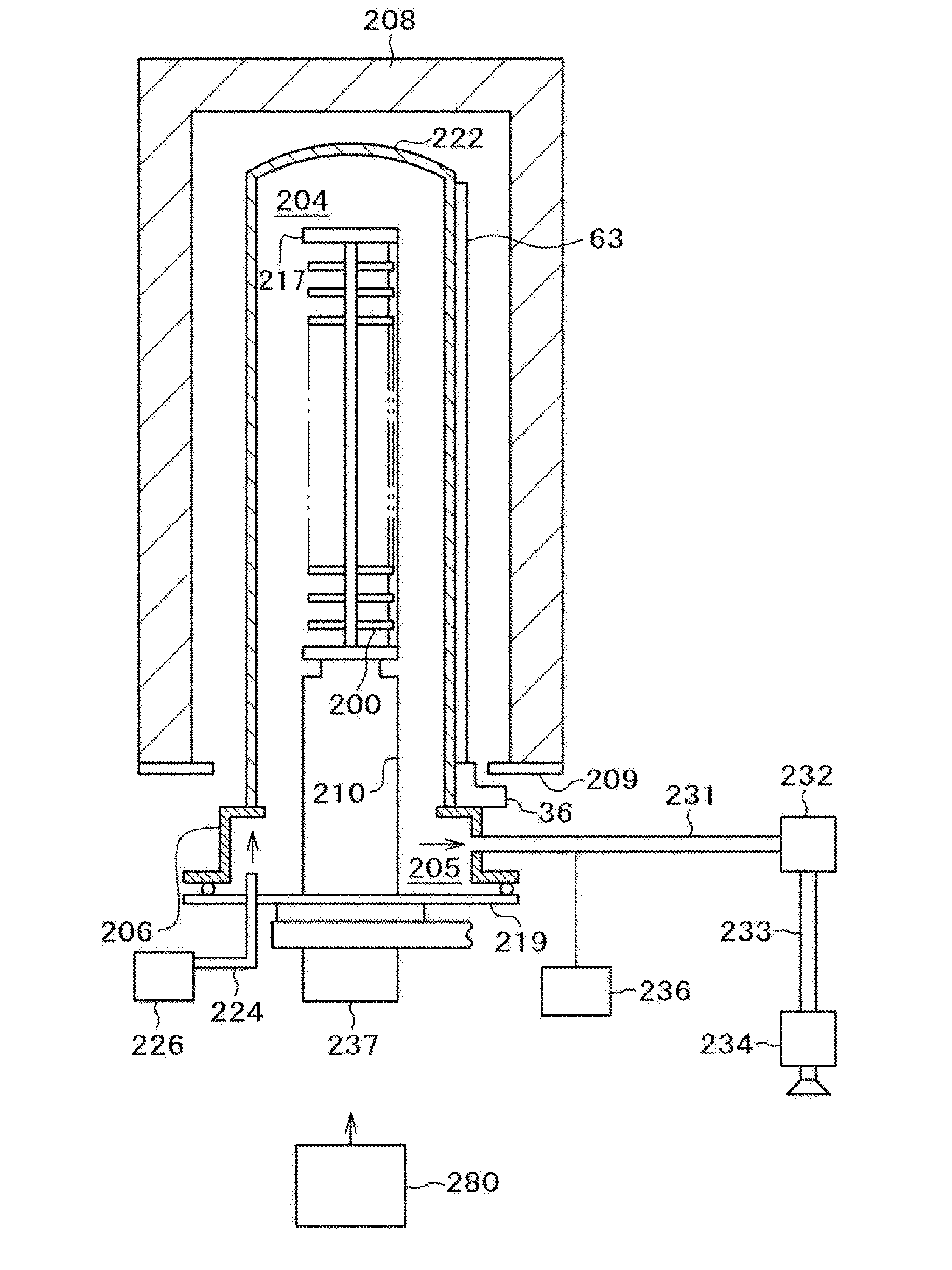
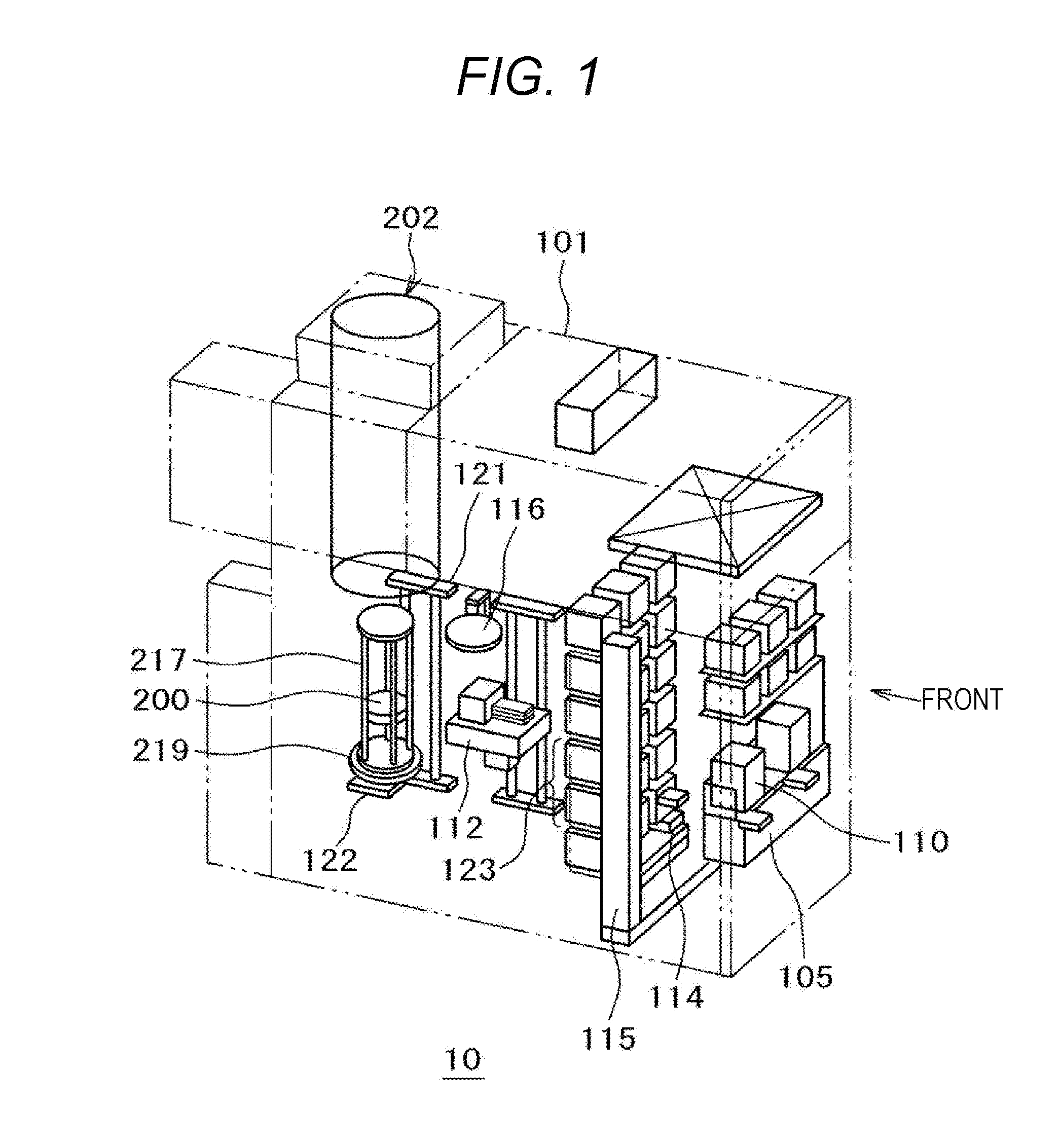
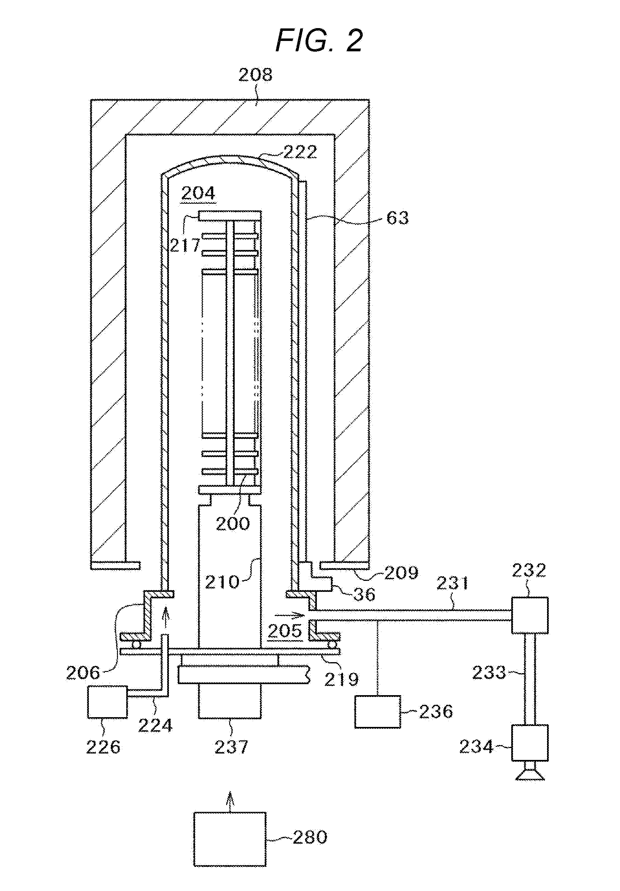
[0044]As a first embodiment of the present invention, an example of a configuration of a substrate processing apparatus that implements a substrate processing process by a heat treatment as one process of a semiconductor device (such as IC) manufacturing process will be described with reference to FIG. 1.

[0045]FIG. 1 is a perspective view of a substrate processing apparatus according to a first embodiment of the present invention. As illustrated in FIG. 1, a substrate processing apparatus 10 according to the first embodiment includes a housing 101 and uses a cassette (pod, also referred to as FOUP) 110 as a wafer carrier (wafer container) to carry a wafer 200, which is a substrate formed of silicon or the like, into and away from the housing 101.

[0046]A cassette stage 105 is installed at a front side of the housing 101. By an in-process carrying device (not illustrated) outside the housing 101, the cassettes 110 are carried and placed onto the cassette stage 105 and carried away fro...

second embodiment

[0120]Subsequently, a structure of the reaction tube thermocouple according to the second embodiment will be described with reference to FIGS. 9 and 10. FIG. 9 is a view illustrating a processing furnace and a thermocouple according to the second embodiment of the present invention. FIG. 10 is a view illustrating a reaction tube thermocouple support structure according to the second embodiment of the present invention. FIG. 10(a) is a view illustrating a configuration of a specific example of a reaction tube thermocouple support structure 400 according to the second embodiment; FIG. 10(b) is a front view of a cut portion 410 to be described later; FIG. 10(c) is a side view of the cut portion 410; and FIG. 10(d) is a schematic view illustrating the attachment of the reaction tube thermocouple support structure 400 to the reaction tube 222. Also, since a substrate processing operation and configurations other than the reaction tube and the reaction tube thermocouple support structure ...

third embodiment

[0137]In the third embodiment, the reaction tube thermocouple protection 63 is divided in the longitudinal direction (vertical direction), and the divided reaction tube thermocouple protections 63 have different thicknesses. That is, the reaction tube thermocouple protections 63 are divided corresponding to the reaction tube thermocouples 53 and are provided separately from each other, and the divided reaction tube thermocouple protections 63 have different thicknesses. Also, since a substrate processing operation and configurations other than the reaction tube and the reaction tube thermocouple support structure are identical to those of the first embodiment, a description thereof will be omitted herein.

[0138]As a result of the research by the inventors, it can be seen that, since the profile thermocouples 52a to 52e have different temperature characteristics, better results are obtained when the wall surfaces constituting the reaction tube thermocouple protections 63 located at po...


PUM

PropertyMeasurementUnit
thicknessaaaaaaaaaa
sizeaaaaaaaaaa
thicknessaaaaaaaaaa

Abstract

A substrate processing apparatus includes: a reaction tube configured to accommodate a substrate holder holding a plurality of substrates and process a substrate held on the substrate holder; a heating unit installed outside the reaction tube and configured to heat an inside of the reaction tube; a protection tube installed to extend in a vertical direction in contact with an outer wall of the reaction tube; an insulating tube disposed inside the protection tube and having through-holes extending in a vertical direction; a thermocouple having a thermocouple junction provided at an upper end thereof, and thermocouple wires joined at the thermocouple junction and inserted into the through-holes of the insulating tube; a gas supply unit configured to supply a gas, for processing a substrate accommodated in the reaction tube, into the reaction tube; and an exhaust unit configured to exhaust a gas from the reaction tube.

Description

BACKGROUND[0001]1. Technical Field[0002]The present invention relates to heat treatment technology for accommodating a substrate in a processing chamber and processing the substrate while heating the substrate. For example, the present invention relates to a temperature detecting method, a substrate processing apparatus, a substrate processing method, and a semiconductor device manufacturing method, which are used to perform heat treatment, such as oxidation processing or diffusion processing, reflow processing or anneal processing for planarization or activation of carriers after ion implantation, film formation processing by thermal chemical vapor deposition (CVD) reaction, on a semiconductor substrate (for example, a semiconductor wafer) in which a semiconductor integrated circuit device (so-called semiconductor device, hereinafter referred to as IC) is formed.[0003]2. Description of the Related Art[0004]In manufacturing an IC, a batch type vertical heat treatment apparatus is wi...

Claims


Application Information

Patent Timeline
Patent Type & Authority Applications(United States)
IPC IPC(8): H01L21/67H01L21/66G01K7/02
CPCH01L21/67098G01K7/02H01L21/67109H01L22/26H01L21/67248H01L2924/0002H01L2924/00
Inventor YAMAGUCHI, HIDETOKOSUGI, TETSUYAUENO, MASAAKI
Owner KOKUSA ELECTRIC CO LTD
Why Eureka
Try Eureka