Method for producing organic light-emitting element

a technology of organic light-emitting elements and manufacturing methods, which is applied in the direction of basic electric elements, electrical equipment, and semiconductor devices, etc., can solve the problems of difficult to precisely adjust the position of the mask used in the vapor deposition method, the difficulty of manufacturing a properly functioning display, and the difficulty of vapor deposition type organic el elements to full-color, large-sized organic el panels with display sizes of around 100 inches, etc., to achieve excellent hole injection characteristics, reduction film thickness reduction

Active Publication Date: 2014-05-08
JOLED INC
View PDF1 Cites 14 Cited by
  • Summary
  • Abstract
  • Description
  • Claims
  • Application Information

AI Technical Summary

Benefits of technology

[0024]Through much devotion and consideration, the inventors of the present invention (hereinafter referred to as “present inventors”) have found that when formed under predetermined film forming conditions, a tungsten oxide layer is provided with improved hole injection characteristics due to an occupied energy level being formed at a binding energy level relatively close to the Fermi surface of the tungsten oxide. In addition, the present inventors have also found that, by firing the tungsten oxide layer so formed under predetermined, strictly-defined conditions, the film density of the tungsten oxide layer increases compared to before the firing is performed, and thus the dissolution resistance of the tungsten oxide layer with respect to the etching solution, the cleaning liquid, etc., that are used during the bank forming process is improved. Based on such findings, the present inventors have arrived at one aspect of the present invention, which reduces an amount of the film thickness reduction and provides, as the hole injection layer, a tungsten oxide layer having excellent hole injection characteristics. Thus, an organic light-emitting element manufactured according to the method pertaining to one aspect of the present invention drives at low voltage and has excellent light-emission efficiency.
[0025]As already described above, the method pertaining to one aspect of the present invention reduces the film thickness reduction amount of the hole injection layer. Accordingly, when manufacturing an organic EL panel in which a plurality of the organic light-emitting elements manufactured according to the method pertaining to one aspect of the present invention are disposed, the absolute level of unevenness in terms of film thickness between the hole injection layers included in the manufactured organic EL panel is reduced over the entire panel, and thus the ununiformity of light-emission efficiency between the organic light-emitting elements included in the manufactured organic EL panel is reduced.

Problems solved by technology

However, although vapor deposition type organic EL elements are desirable for use in small-sized organic EL panels, the application of vapor deposition type organic EL elements to, for example, full-color, large-sized organic EL panels having display sizes of around 100 inches is extremely difficult.
Here, when the organic EL panel to be manufactured becomes greater in area, it is difficult to precisely adjust the position of the mask used in the mask vapor deposition method due to reasons such as the difference in thermal expansion coefficients between the mask and a glass substrate.
Hence, manufacturing of a display that operates properly is difficult.
Thus, in principle, an increased amount of power is consumed by the panel.

Method used


Image

  • Method for producing organic light-emitting element
  • Method for producing organic light-emitting element
  • Method for producing organic light-emitting element

Examples


embodiment 1

Structure of Organic EL Element

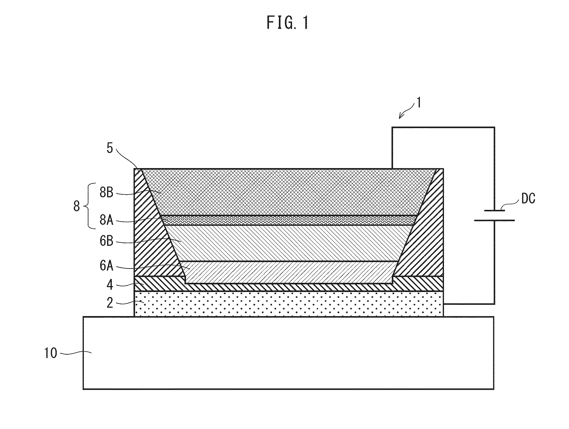
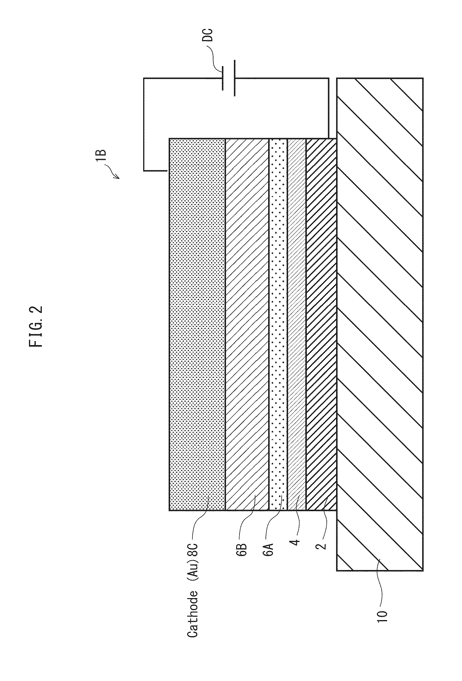
[0087]FIG. 1 is a schematic cross-sectional view illustrating the structure of an organic EL element 1 pertaining to embodiment 1.

[0088]The organic EL element 1 is an application type organic EL element. As such, the organic EL element 1 includes one or more functional layers having been formed by applying functional layer material by wet processing. The organic EL element 1 includes: a hole injection layer 4; one or more functional layers each containing organic material and having a predetermined function; and a pair of electrodes, composed of an anode 2 and a cathode 8. The hole injection layer 4 and the set of one or more functional layers, a buffer layer 6A and a light-emitting layer 6B in this example, are disposed one on top of the other, and are disposed between the pair of electrodes.

[0089]In specific, the organic EL element 1 includes, as illustrated in FIG. 1, a substrate 10, and the anode 2, the hole injection layer 4, the buffer layer 6A, ...

embodiment 2

Overall Structure of Organic EL Element 1C

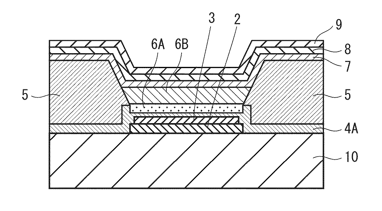
[0269]FIG. 24A is a schematic cross-sectional view illustrating the structure of an organic EL element 1C according to the present embodiment. FIG. 24B is a partially expanded view near a hole injection layer 4C.

[0270]The organic EL element 1C is, for example, an application type organic EL element including one or more functional layers each having been formed by applying material in wet processing. The hole injection layer 4A and a set of one or more functional layers, each containing organic material and having a predetermined function, are disposed one on top of the other, and are disposed between a pair of electrodes, composed of an anode 2 and a cathode 8D.

[0271]Specifically, the organic EL element 1C includes a substrate 10 having the following layered on one main surface thereof in the stated order: the anode 2, an ITO layer 3, the hole injection layer 4A, a buffer layer 6A, a light-emitting layer 6B, an electron injection layer 7, a...


PUM

PropertyMeasurementUnit
total pressureaaaaaaaaaa
temperatureaaaaaaaaaa

Abstract

Method for manufacturing organic EL element including anode, hole injection layer, buffer layer, light-emitting layer, and cathode, layered on substrate in the stated order, and banks defining a light-emission region, and having excellent light-emission characteristics, due to the hole injection layer having excellent hole injection efficiency, being a tungsten oxide layer including an oxygen vacancy structure, formed under predetermined conditions to have an occupied energy level within a binding energy range from 1.8 eV to 3.6 eV lower than a lowest binding energy of a valence band, and after formation, subjected to atmospheric firing at a temperature within 200° C.-230° C. inclusive for a processing time of 15-45 minutes inclusive to have increased film density and improved dissolution resistance against an etching solution, a cleaning liquid, etc., used in a bank forming process.

Description

TECHNICAL FIELD[0001]The present invention relates to a method for manufacturing an organic light-emitting element (referred to hereinafter as an “organic EL element”), which is an electric light-emitting element. Particularly, the present invention relates to a technology for driving such an organic EL element at low electricity while ensuring a wide range of luminous intensity from low luminous intensity to high luminous intensity for the use as a light source or the like.DESCRIPTION OF THE RELATED ART[0002]In recent years, progress is being made in the research and development of various functional elements that utilize organic semiconductors.[0003]An organic EL element is a typical example of such a functional element. An organic EL element is a current-driven light-emitting element, and typically includes a pair of electrodes, composed of an anode and a cathode, and one or more functional layers each containing organic material disposed between the pair of electrodes. In the pr...

Claims


Application Information

Patent Timeline
Patent Type & Authority Applications(United States)
IPC IPC(8): H01L51/56H01L51/50
CPCH01L51/5088H01L51/56H10K50/17H10K71/00H10K59/122
Inventor YAMADA, RYUUTAOHUCHI, SATORUKOMATSU, TAKAHIROFUJIMURA, SHINYAFUJITA, HIROFUMI
Owner JOLED INC
Why Eureka
Try Eureka