Substrate structure having component-disposing area and manufacturing process thereof

a technology of substrate structure and manufacturing process, which is applied in the direction of manufacturing tools, chemistry apparatus and processes, paper/cardboard articles, etc., can solve the problems of increasing the fabrication difficulty of circuit substrates having components and complex processes, and achieves a simple process and a higher production yield rate

Active Publication Date: 2014-05-22
UNIMICRON TECH CORP
View PDF28 Cites 23 Cited by
  • Summary
  • Abstract
  • Description
  • Claims
  • Application Information

AI Technical Summary

Benefits of technology

[0007]Accordingly, the disclosure is directed to a substrate structure having a component-disposing area, which has simpler process and higher production yield rate.
[0008]The disclosure is also directed to a process for a substrate having a component-disposing area, which has simpler steps and higher product yield rate.
[0019]Based on the depiction above, in the disclosure, the dielectric layers are substituted for the solder mask layer disposed on the core layer within the component-disposing area in the prior art, so that, in the disclosure, the dielectric layers located on the inside and the outside of the component-disposing area can be integrally and simultaneously formed, which simplifies the conventional complicated substrate process. In addition, in the disclosure, a laser-resistant metallic pattern is disposed on the dielectric layer for preventing the laser drilling from penetrating through the dielectric layer, unlike the prior art where the laser-resistant metallic pattern and the pads are together disposed on the core layer so as to avoid the difficulty in the laser drilling depth control. In short, the disclosure certainly simplifies the process for a substrate having a component-disposing area and advances the product yield rate.

Problems solved by technology

In particular, the process should be performed separately from other processes of the circuit substrate, which makes the process more complicated.
All the above-mentioned issues increase the fabrication difficulty of the circuit substrate having components disposed therein.
In addition, since the thickness of a core layer is usually less than 100 microns (μm), which is also a great challenge for today's solder-resist fabrication.

Method used


Image

  • Substrate structure having component-disposing area and manufacturing process thereof
  • Substrate structure having component-disposing area and manufacturing process thereof
  • Substrate structure having component-disposing area and manufacturing process thereof

Examples


Embodiment Construction

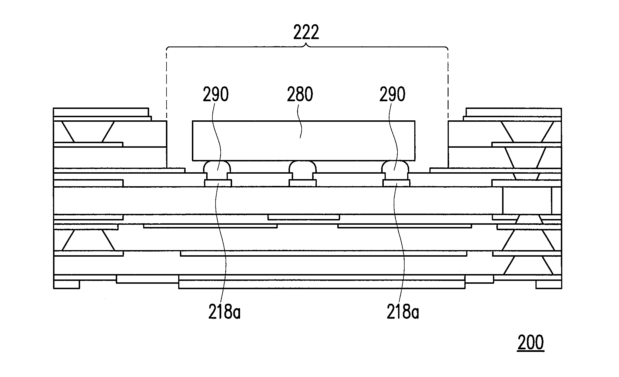
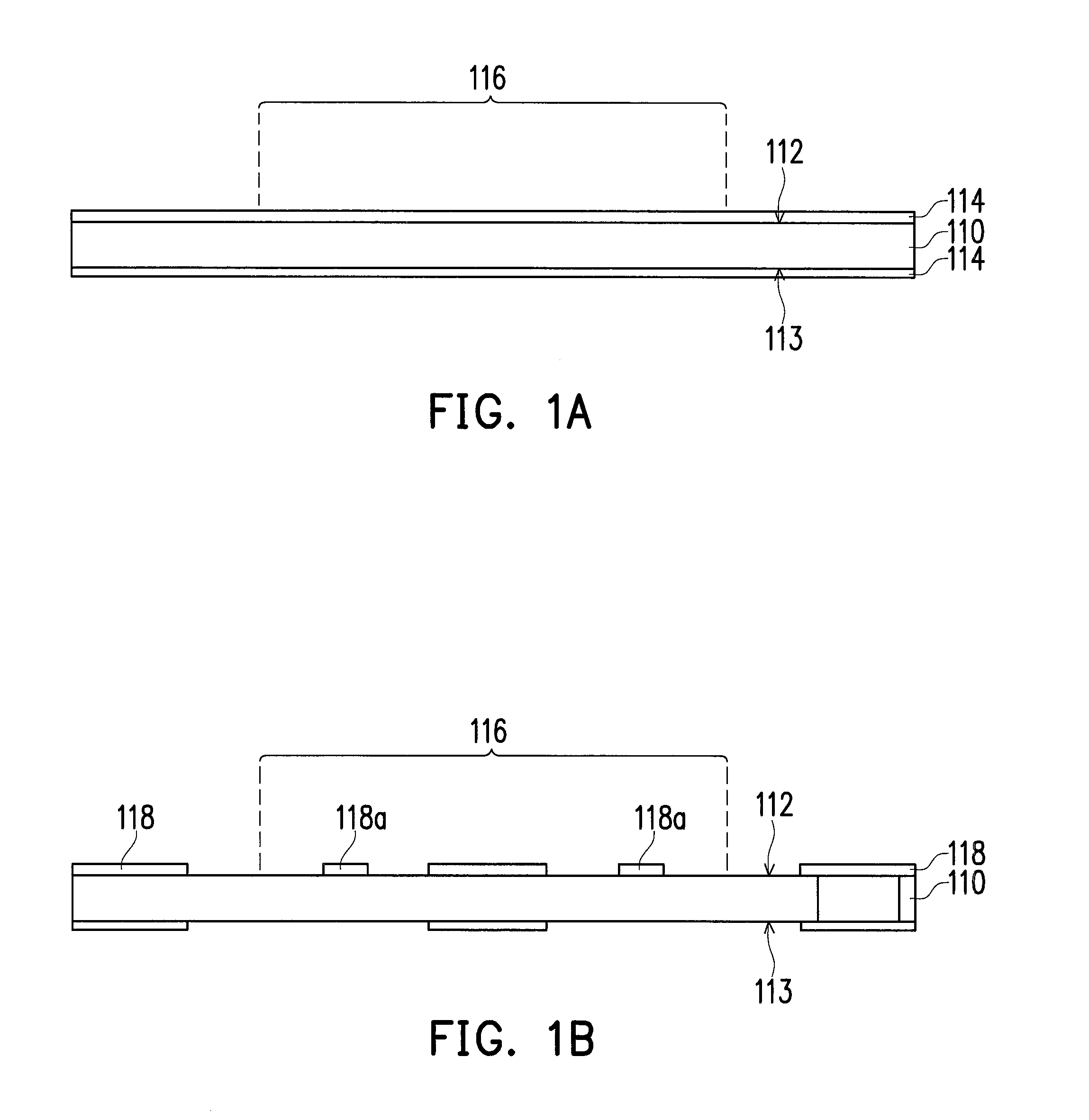
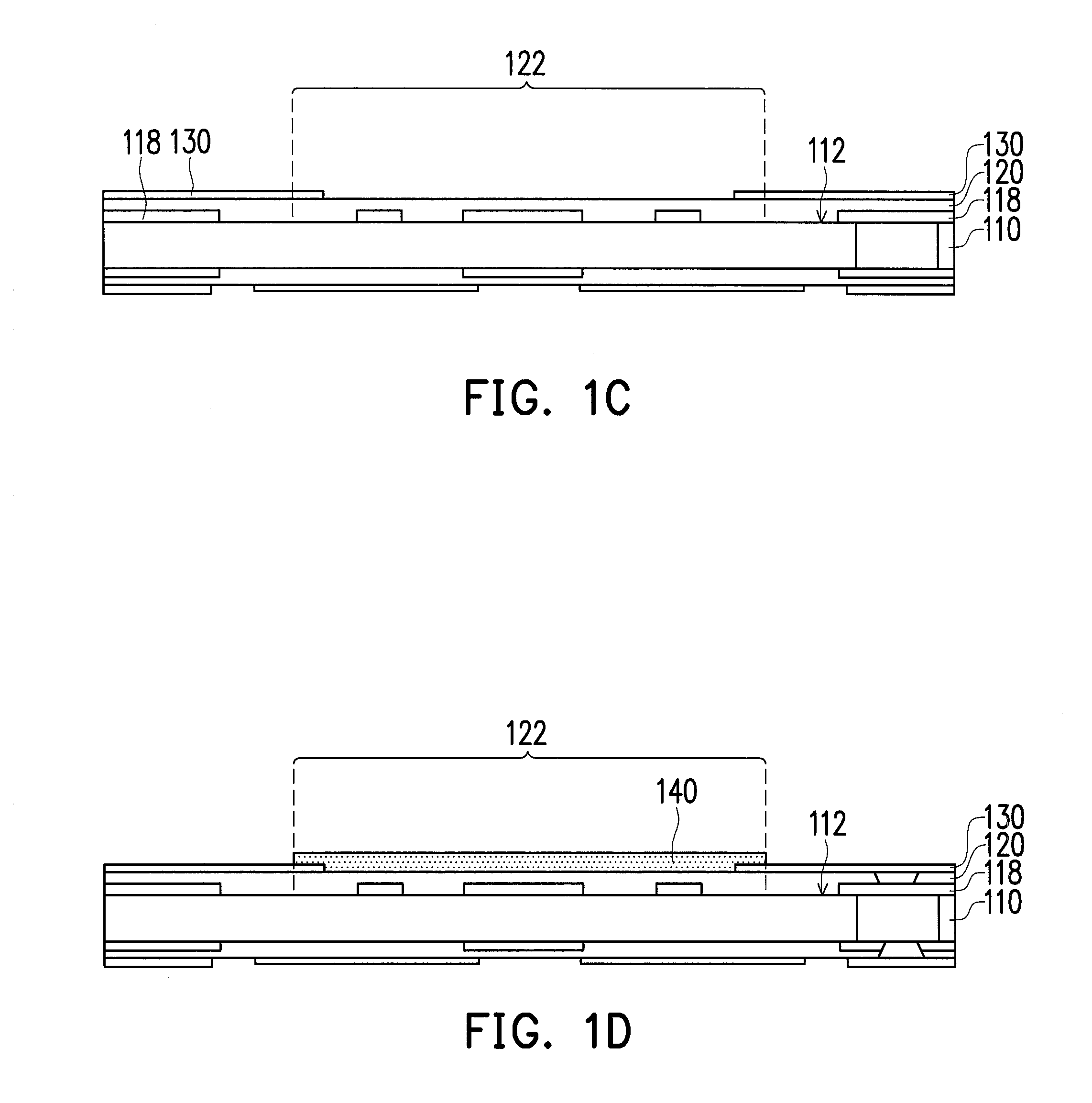
[0023]FIGS. 1A-1H are cross-sectional diagrams showing a manufacturing process of a substrate having a component-disposing area according to an embodiment of the disclosure. Referring to FIG. 1A, a manufacturing process of a substrate having a component-disposing area in the embodiment includes following steps. First, a core layer 110 shown by FIG. 1A including a first surface 112, a metallic layer 114 and a component-disposing area 116 is provided. The metallic layer 114 is disposed on the first surface 112 and the component-disposing area 116 is an area on the surface of the core layer 110 for disposing an electronic component. It should be noted that, in the embodiment, the core layer 110 is a bi-surfaces copper foil core layer, i.e., the two opposite surfaces (the first surface 112 and a second surface 113 opposite to each other) of the core layer 110 respectively have two copper foils (the metallic layer 114 as shown by FIG. 1A), and circuit layers are simultaneously fabricated...


PUM

PropertyMeasurementUnit
thicknessaaaaaaaaaa
areaaaaaaaaaaa
penetrating depthaaaaaaaaaa

Abstract

A substrate structure having a component-disposing area and a process thereof are provided. The substrate structure having a component-disposing area includes a core layer, a first dielectric-layer, a laser-resistant metallic-pattern and a second dielectric-layer. The core layer includes a first surface, a component-disposing area and a patterned metallic-layer disposed on the first surface and including multiple pads, and the pads are located within the component-disposing area. The first dielectric-layer is disposed on the core layer and includes multiple openings to respectively expose the pads. The laser-resistant metallic-pattern is disposed on the first dielectric-layer and surrounds a projection area of the first dielectric-layer which the component-disposing area is orthogonally projected on. The second dielectric-layer is disposed on the first dielectric-layer and covers the laser-resistant metallic-pattern, the second dielectric-layer includes a component-disposing cavity corresponding to the projection area, penetrating through the second dielectric-layer and communicated with the openings to expose the pads.

Description

CROSS-REFERENCE TO RELATED APPLICATION[0001]This application claims the priority benefit of Taiwan application serial no. 101143499, filed on Nov. 21, 2012. The entirety of the above-mentioned patent application is hereby incorporated by reference herein and made a part of this specification.BACKGROUND[0002]1. Field of the Disclosure[0003]The disclosure generally relates to a substrate structure and a manufacturing process thereof, and more particularly, to a substrate structure having a component-disposing area and a manufacturing process thereof.[0004]2. Description of Related Art[0005]In recent years, with ever-changing advances in electronic technology, high-tech electronics industry appeared one after another, which makes the more humanized and better in function electronic products continue to be launched. And these electronic products are developing toward the light, thin, short and small figure design. Usually in these electronic products, a circuit substrate is disposed for...

Claims


Application Information

Patent Timeline
Patent Type & Authority Applications(United States)
IPC IPC(8): H05K1/11H05K1/09H05K13/04
CPCH01L21/4857H01L23/13H01L23/49822H01L24/32H01L24/48H01L2224/16225H01L2224/32225H01L2224/48091H01L2224/48227H01L2224/48228H01L2224/73265H01L2924/00014H01L2924/12042H01L2924/15153H01L2924/15333H05K1/183H05K3/4697H05K2201/09127H01L2924/00H01L2224/45015H01L2924/207H01L2224/45099H01L24/81H01L24/85H01L2924/1517H01L2924/37001
Inventor CHANG, CHENG-JUIWU, MING-HAO
Owner UNIMICRON TECH CORP
Why Eureka
Try Eureka