
Method to Improve Charge Trap Flash Memory Core Cell Performance and Reliability

a technology of core cell and charge trap, which is applied in the field of memory fabrication, can solve the problems of poor quality, and top oxide, and achieve satisfactory flash memory cell performance and reliability, and degraded flash memory cell performance

Active Publication Date: 2014-05-22
MONTEREY RES LLC +1
View PDF0 Cites 0 Cited by
  • Summary
  • Abstract
  • Description
  • Claims
  • Application Information

AI Technical Summary

Benefits of technology

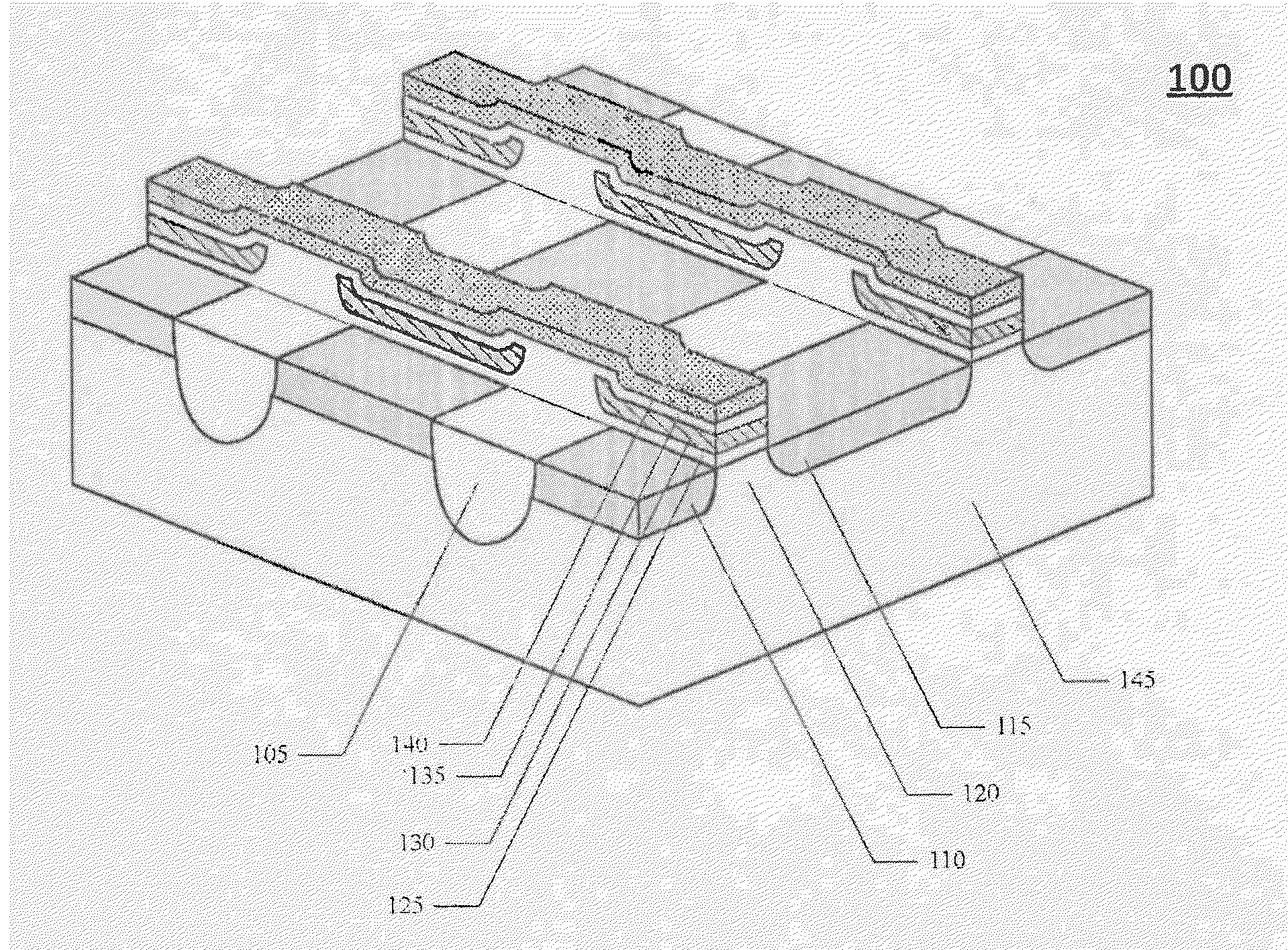
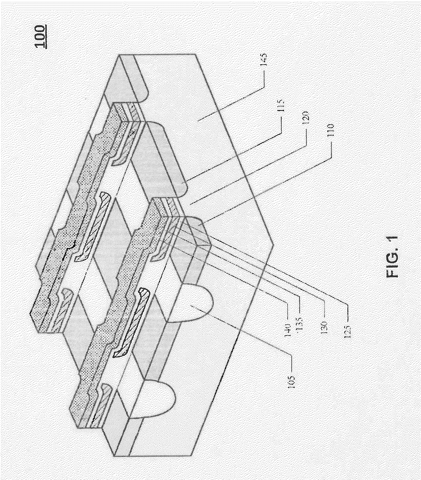
The patent text describes a method for manufacturing a flash memory cell with a top oxide layer that maintains satisfactory performance and reliability. The method involves forming a tunneling dielectric layer, a charge trapping layer, and multiple trench isolation regions. A blocking dielectric layer is then oxidized and a polysilicon region is formed on top. This process ensures that the top oxide layer is properly manufactured without compromising the performance of the flash memory cell.

Problems solved by technology

Degraded flash memory cell performance can result from top oxide issues such as “corner thinning” and poor quality.

Method used


Image

  • Method to Improve Charge Trap Flash Memory Core Cell Performance and Reliability
  • Method to Improve Charge Trap Flash Memory Core Cell Performance and Reliability
  • Method to Improve Charge Trap Flash Memory Core Cell Performance and Reliability

Examples


Embodiment Construction

[0019]This specification discloses one or more embodiments that incorporate the features of this invention. The disclosed embodiment(s) merely exemplify the invention. The scope of the invention is not limited to the disclosed embodiment(s). The invention is defined by the claims appended hereto.

[0020]The embodiment(s) described, and references in the specification to “one embodiment”, “an embodiment”, “an example embodiment”, etc., indicate that the embodiment(s) described may include a particular feature, structure, or characteristic, but every embodiment may not necessarily include the particular feature, structure, or characteristic. Moreover, such phrases are not necessarily referring to the same embodiment. Further, when a particular feature, structure, or characteristic is described in connection with an embodiment, it is understood that it is within the knowledge of one skilled in the art to effect such feature, structure, or characteristic in connection with other embodimen...


PUM


Abstract

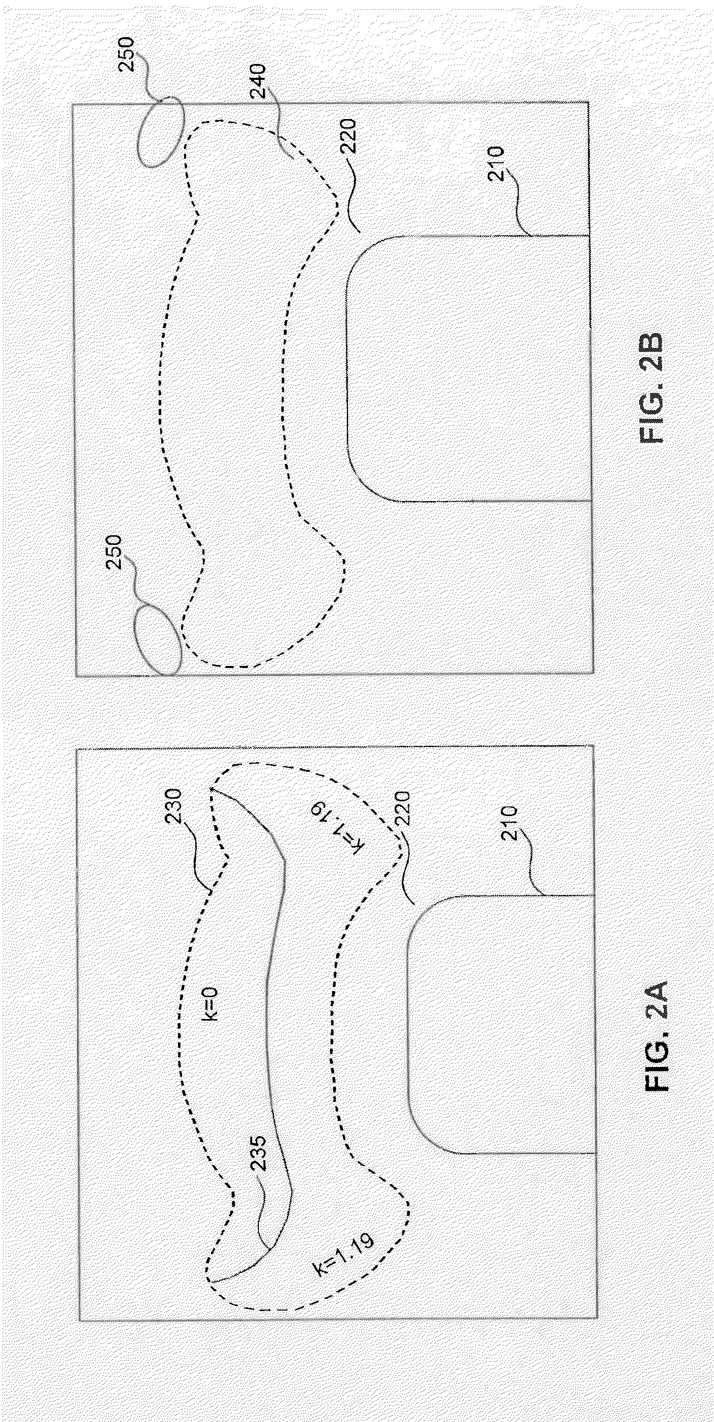
A semiconductor processing method to provide a high quality bottom oxide layer and top oxide layer in a charged-trapping NAND and NOR flash memory. Both the bottom oxide layer and the top oxide layer of NAND and NOR flash memory determines array device performance and reliability. The method describes overcomes the corner thinning issue and the poor top oxide quality that results from the traditional oxidation approach of using pre-deposited silicon-rich nitride.

Description

BACKGROUND[0001]1. Field[0002]This invention relates generally to memory fabrication, and more particularly to a semiconductor processing method for flash memory fabrication.[0003]2. Background Art[0004]The semiconductor market has been undergoing extensive growth over the past few decades. This trend is expected to continue for the foreseeable future since a large portion of this market is the memory segment. The memory segment can be broadly categorized into two classes, namely volatile memory and non-volatile memory. Volatile memory such as SRAM and DRAM lose their data content when the power supply is removed. In contrast, non-volatile memories such as EEPROM and flash memories maintain their data content after the power supply has been removed.[0005]Non-volatile memories offer particular advantages, and thereby support a wide range of applications including computer, automotive and consumer electronic devices. Flash memory is a non-voltage memory that can be electrically erased...

Claims


Application Information

Patent Timeline
Patent Type & Authority Applications(United States)
IPC IPC(8): H01L21/762H10B69/00
CPCH01L21/762H01L21/76232H01L21/3081H01L29/4234H01L29/66833H01L29/40117H01L29/513H01L29/792H10B43/30
Inventor CHEN, TUNG-SHENGFANG, SHENQING
Owner MONTEREY RES LLC
Learn More