Wafer processing method

a processing method and k film technology, applied in welding/soldering/cutting articles, metal working devices, manufacturing tools, etc., can solve the problems of difficult cutting of substrate and k film by using cutting blades, affecting the quality of k film, and causing fatal damage to devices, so as to reduce the die strength of each device

Active Publication Date: 2014-05-22
DISCO CORP
View PDF4 Cites 26 Cited by
  • Summary
  • Abstract
  • Description
  • Claims
  • Application Information

AI Technical Summary

Benefits of technology

[0007]However, in forming the laser processed groove along each street of the semiconductor wafer to thereby remove the functional layer along each street, a modified layer is formed on the upper surface of the substrate of the semiconductor wafer along each street. Accordingly, even when the substrate is cut along each street (laser processed groove) by using the cutting blade, the modified layer is left on the opposite sides of each street. That is, the modified layer is left along the peripheral edge of each device on the front side of the substrate, causing a reduction in die strength of each device.
[0008]It is therefore an object of the present invention to provide a wafer processing method which can reliably divide a wafer into the individual devices along the streets without a reduction in die strength of each device, wherein the wafer includes a substrate and a functional layer formed on the front side of the substrate and the devices are formed from the functional layer.
[0013]According to the present invention, the modified layer formed on the opposite sides of each street in the functional layer removing step is etched off by performing the plasma etching step, so that the die strength of each device can be improved. Furthermore, each division groove is formed by plasma etching, so that chipping due to the use of a cutting blade can be avoided to thereby further improve the die strength of each device.

Problems solved by technology

The Low-k film is different in material from the substrate constituting the wafer, so that it is difficult to cut the substrate together with the Low-k film by using the cutting blade.
That is, the Low-k film is very brittle like mica.
Accordingly, when the semiconductor wafer having the Low-k film is cut along the streets by using the cutting blade, there arises a problem such that the Low-k film may be separated and this separation may reach the circuits to cause fatal damage to the devices.

Method used


Image

  • Wafer processing method
  • Wafer processing method
  • Wafer processing method

Examples


Embodiment Construction

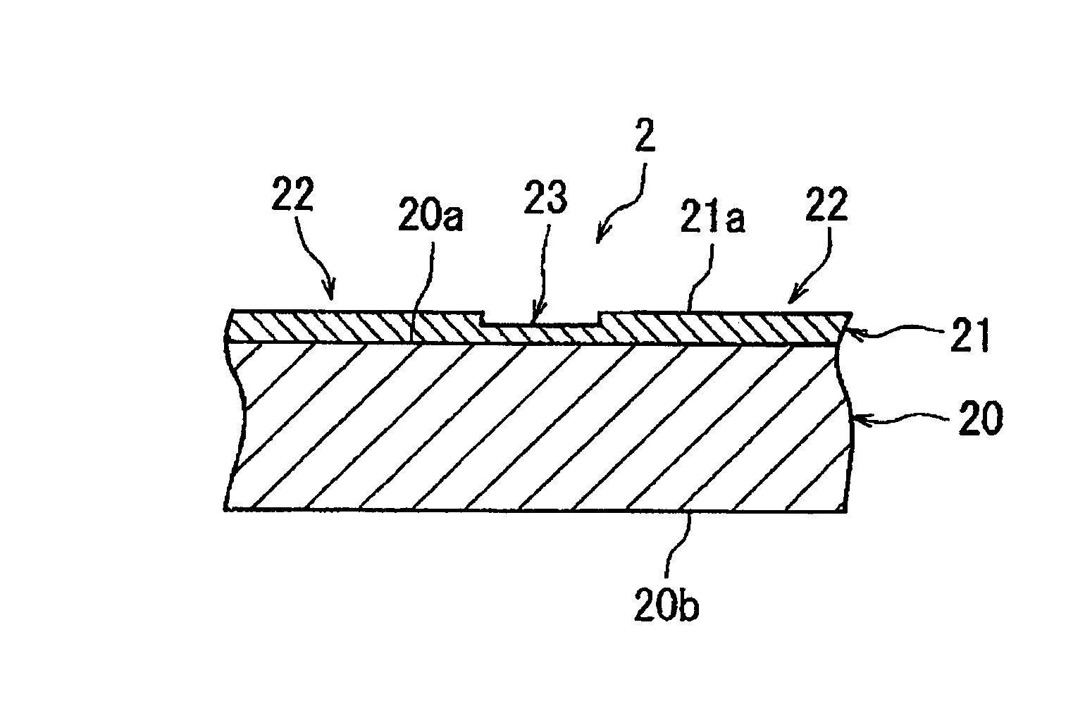
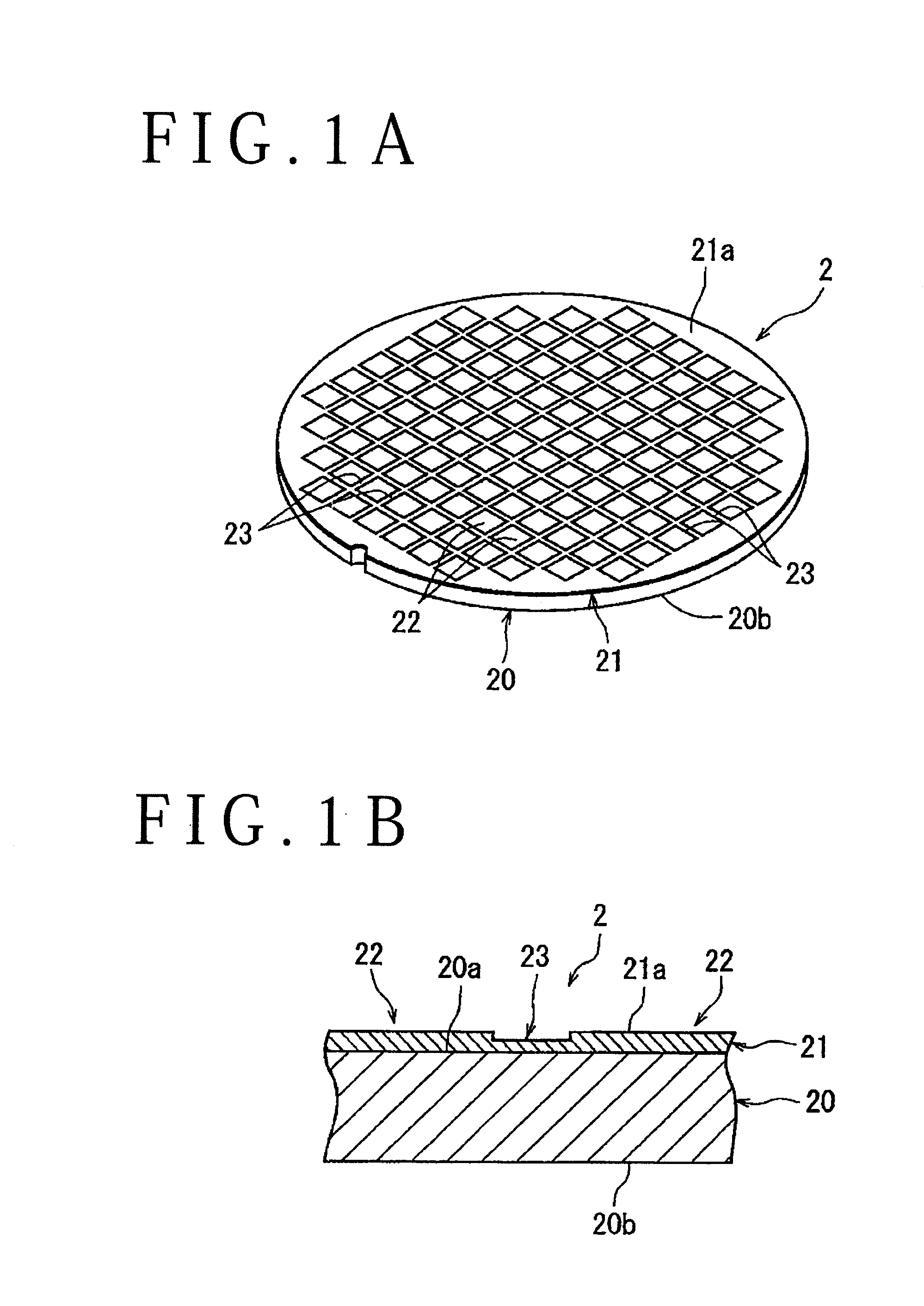
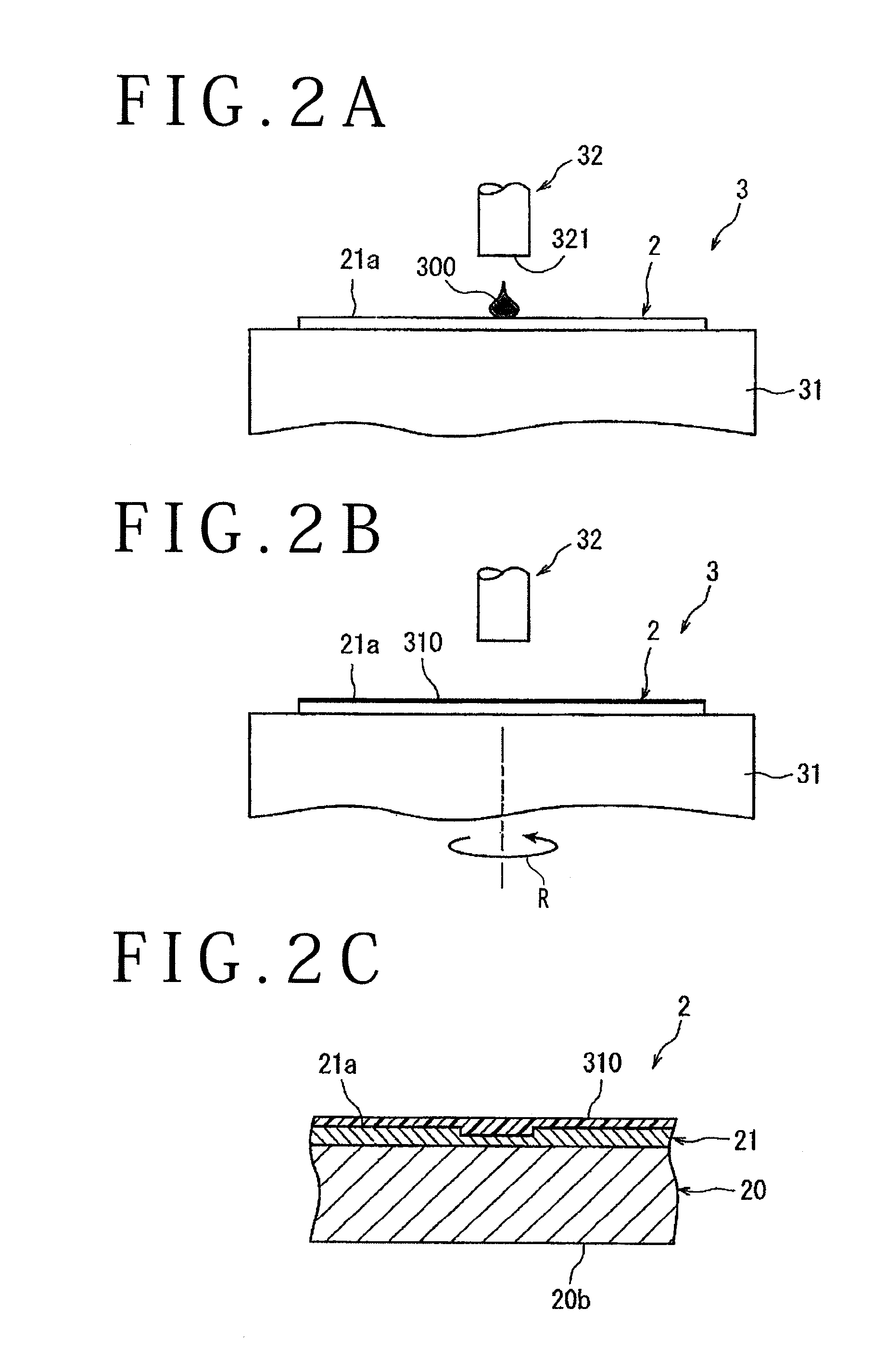
[0026]The wafer processing method according to the present invention will now be described in more detail with reference to the attached drawings. FIG. 1A is a perspective view of a semiconductor wafer 2 to be divided into individual devices by the wafer processing method according to the present invention, and FIG. 1B is an enlarged sectional view of an essential part of the semiconductor wafer 2 shown in FIG. 1A. As shown in FIGS. 1A and 1B, the semiconductor wafer 2 is composed of a silicon substrate 20 and a functional layer 21 formed on the front side 20a of the silicon substrate 20. For example, the silicon substrate 20 has a thickness of 725 μm and a diameter of 200 mm. The functional layer 21 is composed of an insulating film and a functional film formed on the insulating film, the functional film forming a plurality of circuits. A plurality of devices 22 such as ICs and LSIs are formed like a matrix from the functional layer 21. For example, the thickness of the functional ...


PUM

PropertyMeasurementUnit
diameteraaaaaaaaaa
thicknessaaaaaaaaaa
thicknessaaaaaaaaaa

Abstract

A wafer processing method divides a wafer into individual devices along crossing streets formed on the front side of the wafer. The wafer has a substrate and a functional layer formed on the front side of the substrate. The individual devices are formed from the functional layer and are partitioned by the streets. A laser beam is applied along the streets from the front side of the functional layer to thereby remove the functional layer along the streets. A resist film is formed on the front side of the functional layer except on each street. The substrate of the wafer is plasma-etched along each street where the functional layer is absent to the depth corresponding to the finished thickness of each device, thereby forming a division groove along each street and also etching off a modified layer formed on the opposite sides of each street.

Description

BACKGROUND OF THE INVENTION[0001]1. Field of the Invention[0002]The present invention relates to a wafer processing method for dividing a wafer into a plurality of individual devices along a plurality of crossing streets formed on the front side of the wafer, the wafer being composed of a substrate and a functional layer formed on the front side of the substrate, the functional layer being composed of an insulating film and a functional film formed on the insulating film, the individual devices being formed from the functional layer and partitioned by the streets.[0003]2. Description of the Related Art[0004]As well known in the art, in a semiconductor device fabrication process, a functional layer composed of an insulating film and a functional film is formed on the front side of a substrate such as a silicon substrate, and a plurality of devices such as ICs and LSIs are formed like a matrix from this functional layer, thus obtaining a semiconductor wafer having the plural devices. ...

Claims


Application Information

Patent Timeline
Patent Type & Authority Applications(United States)
IPC IPC(8): H01L21/78
CPCB23K26/40B23K26/364B23K2101/40B23K2103/172H01L21/78
Inventor MATSUZAKI, SAKAEARAMI, JUNICHI
Owner DISCO CORP
Why Eureka
Try Eureka