

Ge-Sb-Te FILM FORMING METHOD, Ge-Te FILM FORMING METHOD, AND Sb-Te FILM FORMING METHOD
a technology of te film and forming method, which is applied in the direction of coating, chemical vapor deposition coating, and metallic material coating process, etc., can solve the problems of poor electrical characteristics, low surface smoothness, and short maintenance of high resistance state, and achieve high surface smoothness and electrical characteristics.
- Summary
- Abstract
- Description
- Claims
- Application Information
AI Technical Summary
Benefits of technology
Problems solved by technology
Method used
Image

Examples
first example embodiment
[0114]Now, an example embodiment in which a formation of a Ge—Sb—Te film by ALD can be verified will be explained.
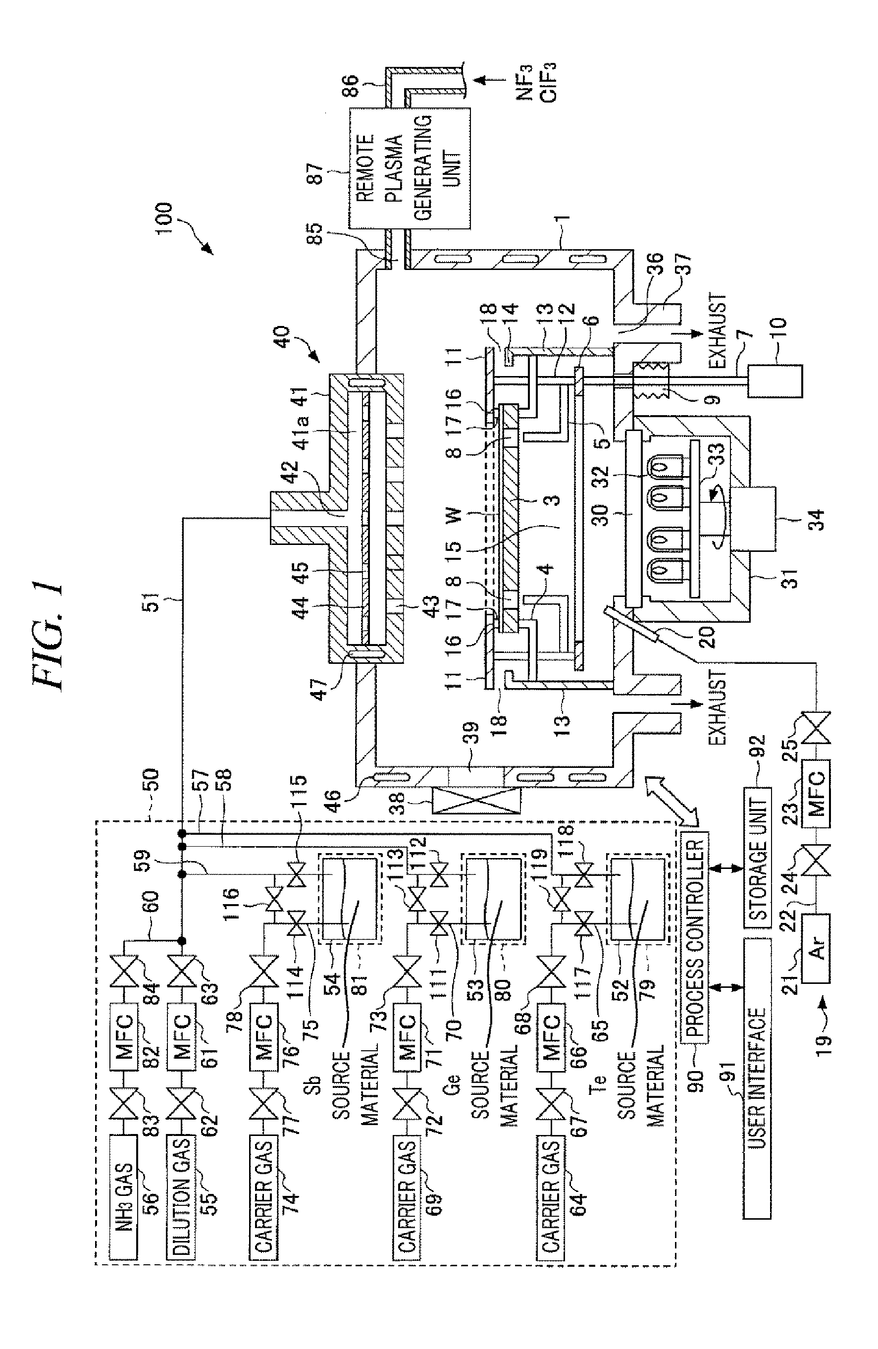
[0115]In the present example embodiment, a temperature of the sidewall of the processing vessel (chamber) 1 is set to be, e.g., about 50° C. to about 60° C. by the cartridge heaters 46. Further, a temperature of the mounting table is set to be, e.g., about 70° C. by adjusting a lamp power in advance, and a wafer W having a diameter of, e.g., about 300 mm is loaded into the processing vessel by using an arm of a transfer robot. Then, a Ge—Sb—Te film is formed in the above-described sequences under the following conditions (see Table 1).
[0116]Furthermore, Ge(OCH3)4 is used as a Ge source material; Sb(OC2H5)3 is used as a Sb source material; and Te(Si(CH3)3)2 is used as a Te source material. Each of these source materials is supplied from the source storage (bottle) heated to a temperature ranging from, e.g., about 30° C. to about 50° C. through a bubbling method by flowing...
second example embodiment
[0159]Except that conditions for forming a Ge—Sb—Te film are changed as follows, a Ge—Sb—Te film is formed through the same processes as those of the first example embodiment (see Table 2).
[0160]Film Forming Conditions:
[0161](Supply of Additive Gas)
[0162]Additive gas (NH3) adding process: see Table 2
[0163]Flow rate ratio of the additive gas (NH3) to a dilution gas (or to an inert gas in a purging process): see Table 2
[0164](Common Conditions for Each Process)
[0165]Chamber pressure: about 800 Pa (about 6 Torr)
[0166]Counter purge flow rate (Te): about 500 mL / min (sccm)
[0167]Counter purge flow rate (Sb): about 100 mL / min (sccm)
[0168]Counter purge flow rate (Ge): about 100 mL / min (sccm)
[0169]Backside Ar gas flow rate: about 200 mL / min (sccm)
[0170]Flow rate of the dilution gas (or the inert gas in the purging process): see Table 2 (for example, about 100 mL / min (sccm))
[0171](i) A Sb source material introducing process of introducing the Sb source material into the processing vessel[0172]...
third example embodiment
[0197]Now, an example for investigating improvement of smoothness and electrical characteristics of a Ge—Sb—Te film obtained by the film forming method by ALD in accordance with the present example embodiment will be explained.
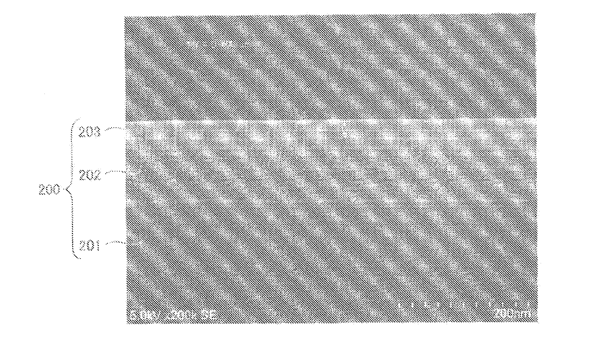
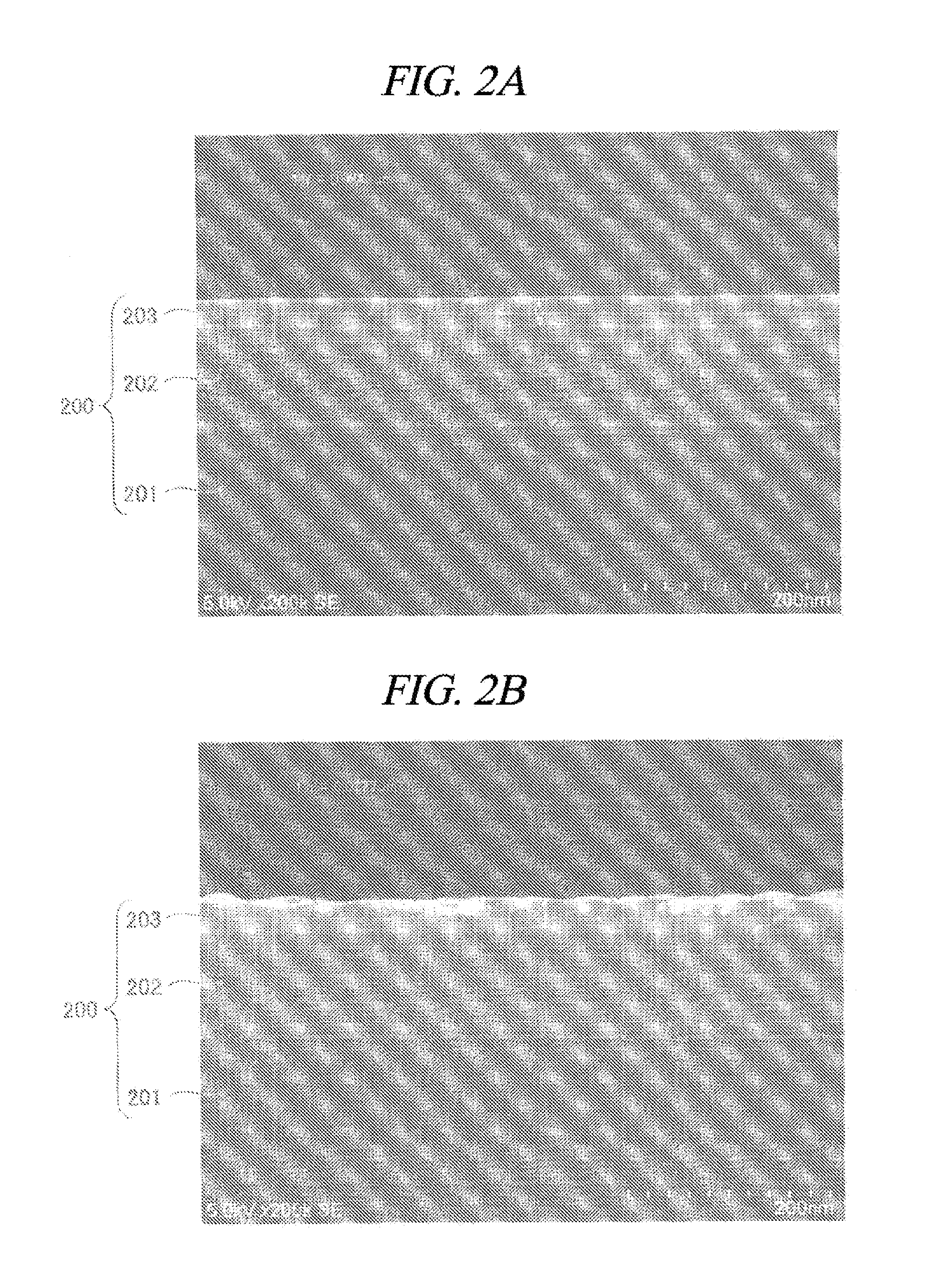
[0198]FIG. 2A and FIG. 2B provide scanning electron microscope (SEM) images for describing smoothness of Ge—Sb—Te films obtained in the present example embodiment. In the present example embodiment, a processing target object 200, which is prepared by forming a silicon oxide film 202 on a silicon wafer 201 and forming a Ge—Sb—Te film 203 on the silicon oxide film 202, is used. FIG. 2A is an SEM image of a Ge—Sb—Te film obtained through the same process as that of the experimental example 16 of Table 2, and FIG. 2B is an SEM image of a Ge—Sb—Te film obtained through the same process as that of the comparative example 1 of Table 1.
[0199]As can be seen from FIG. 2A and FIG. 2B, as compared to the Ge—Sb—Te film obtained by the method of the comparative example, th...
PUM
| Property | Measurement | Unit |
|---|---|---|
| partial pressure | aaaaa | aaaaa |
| carbon number | aaaaa | aaaaa |
| speed | aaaaa | aaaaa |
Abstract
Description
Claims
Application Information