Carbon based nonvolatile cross point memory incorporating carbon based diode select devices and mosfet select devices for memory and logic applications

a nonvolatile cross-point memory, carbon-based technology, applied in nanoinformatics, cycle equipment, instruments, etc., can solve the problems of low fabrication cost and very little power consumption

Active Publication Date: 2014-06-19
NANTERO
View PDF14 Cites 34 Cited by
  • Summary
  • Abstract
  • Description
  • Claims
  • Application Information

AI Technical Summary

Problems solved by technology

A resistive change memory device has resistive change memory elements that are scalable to very high den

Method used


Image

  • Carbon based nonvolatile cross point memory incorporating carbon based diode select devices and mosfet select devices for memory and logic applications
  • Carbon based nonvolatile cross point memory incorporating carbon based diode select devices and mosfet select devices for memory and logic applications
  • Carbon based nonvolatile cross point memory incorporating carbon based diode select devices and mosfet select devices for memory and logic applications

Examples


Embodiment Construction

NRAM and Cross Point Memory Cells

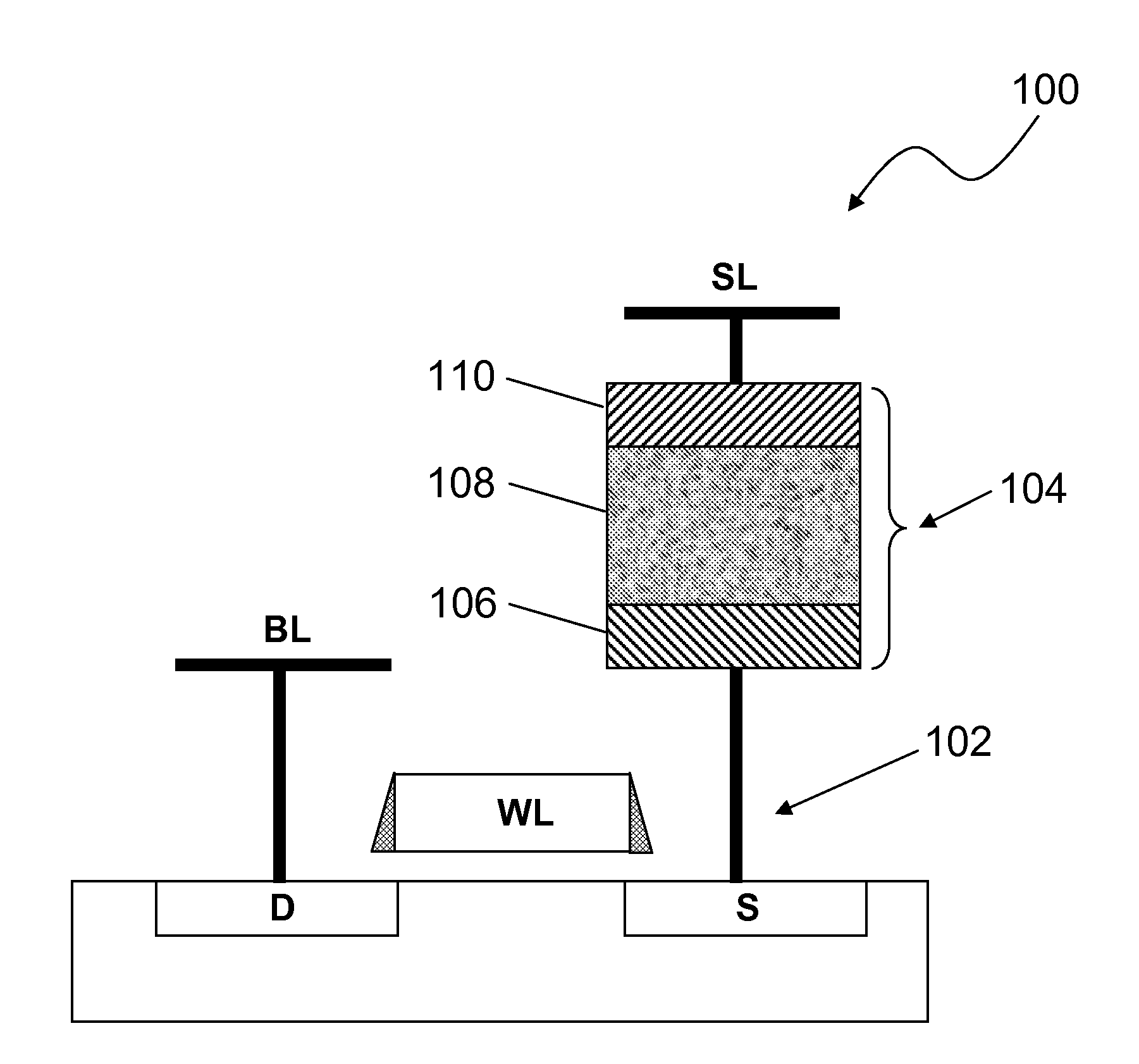
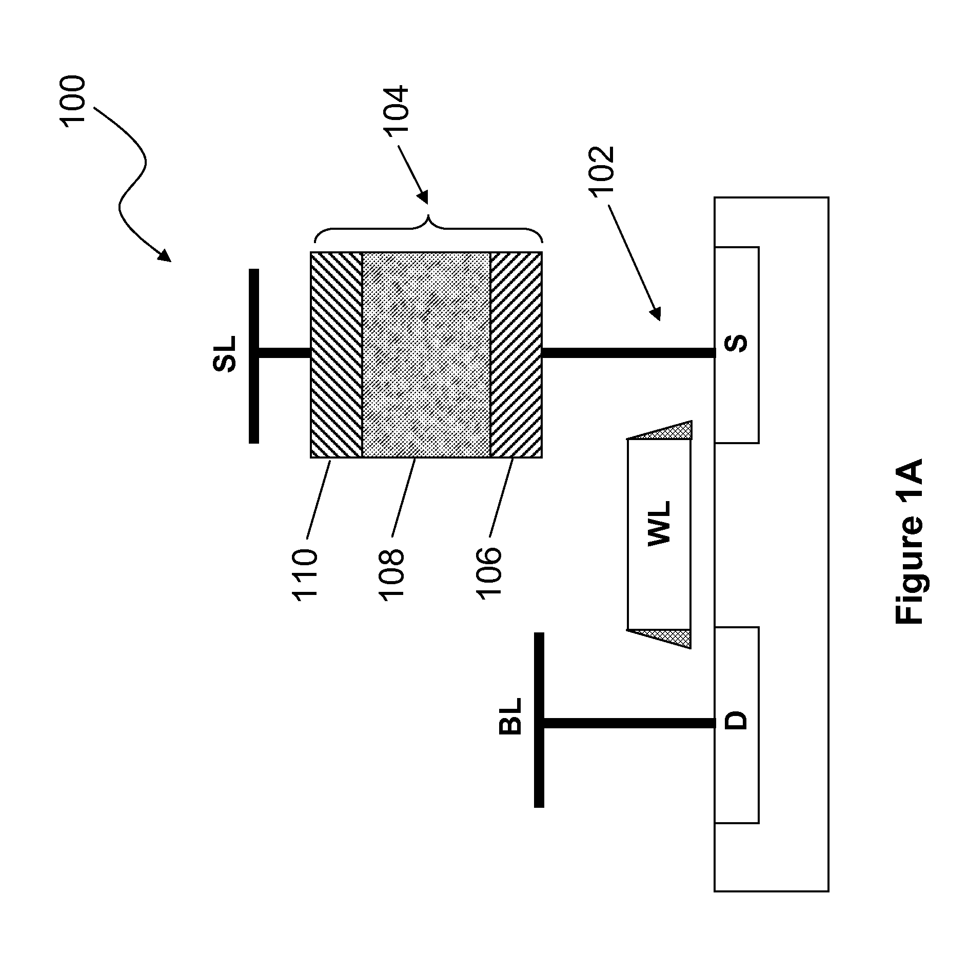
[0168]The present disclosure is generally directed toward nonvolatile resistive change memory cells (or elements) forming 1-R memory cells in a cross point cell configuration, approximately 4F2 in area, with cell select and nonvolatile storage functions combined in a single element. Nonvolatile resistive change memory elements using carbon layers as storage elements can form cross point nonvolatile resistive memory elements. In the present disclosure, the term carbon layer is defined as any allotrope of carbon, excluding amorphous carbon.

[0169]To elaborate further, a carbon layer as referred to herein for the present disclosure includes a layer of multiple, interconnected carbon structures (such as, but not limited to, carbon nanotubes, graphite, buckyballs, and nanocapsules) formed in a layer such as to provide at least one electrically conductive path through the layer. The carbon layer can be, for example, a nanotube fabric (as described in detail...


PUM


Abstract

The present disclosure is directed toward carbon based diodes, carbon based resistive change memory elements, resistive change memory having resistive change memory elements and carbon based diodes, methods of making carbon based diodes, methods of making resistive change memory elements having carbon based diodes, and methods of making resistive change memory having resistive change memory elements having carbons based diodes. The carbon based diodes can be any suitable type of diode that can be formed using carbon allotropes, such as semiconducting single wall carbon nanotubes (s-SWCNT), semiconducting Buckminsterfullerenes (such as C60 Buckyballs), or semiconducting graphitic layers (layered graphene). The carbon based diodes can be pn junction diodes, Schottky diodes, other any other type of diode formed using a carbon allotrope. The carbon based diodes can be placed at any level of integration in a three dimensional (3D) electronic device such as integrated with components or wiring layers.

Description

TECHNICAL FIELD[0001]The present disclosure generally relates to carbon based nonvolatile cross point memory cells using carbon nanotubes, and other carbon allotropes, in corresponding memory arrays. It also relates to carbon based diode select devices formed using carbon nanotubes and other carbon allotropes, carbon based diodes formed as part of cross point memory cells, and carbon based diodes for use with any type of electronic device. It also relates to voltage scaled MOSFET select devices.CROSS-REFERENCE TO RELATED APPLICATIONS[0002]This application is related to the following U.S. patents, which are assigned to the assignee of the present application, and are hereby incorporated by reference in their entirety:[0003]U.S. Pat. No. 6,574,130, filed Jul. 25, 2001, entitled “Hybrid Circuit Having Nanotube Electromechanical Memory;”[0004]U.S. Pat. No. 6,643,165, filed Jul. 25, 2001, entitled “Electromechanical Memory Having Cell Selection Circuitry Constructed with Nanotube Technol...

Claims


Application Information

Patent Timeline
IPC IPC(8): H01L45/00
CPCH01L45/14G11C13/003G11C13/025G11C23/00H01L29/861H01L29/872H01L29/1606G11C2213/35G11C2213/71G11C2213/72G11C2213/77G11C2213/79H01L29/0669B82Y10/00G11C13/0002H10B63/20H10B63/84H10B63/845H10N70/20H10N70/823H10N70/826H10N70/8845H10N70/021H10N70/063H10K19/202H10K85/221H10K10/23H10B63/80H10N70/043B62J7/06G11C13/0069G11C13/0097
Inventor BERTIN, CLAUDE L.CLEAVELIN, C. RINNRUECKES, THOMASHUANG, X. M. HENRYMANNING, H. MONTGOMERY
Owner NANTERO
Why Eureka
Try Eureka