Quantifying silicon degradation in an integrated circuit

a technology of integrated circuits and silicon degradation, which is applied in the direction of generating/distributing signals, pulse techniques, instruments, etc., can solve the problems of reducing the intrinsic speed of an affected sub-circuit and component, waste of power consumption, and unnecessarily slow performance for a large amount of the lifetime of the ic device, so as to reduce voltage margins, improve computing performance, and accurate measurement of semiconductor degradation over time

Inactive Publication Date: 2014-06-26
NVIDIA CORP
View PDF2 Cites 34 Cited by
  • Summary
  • Abstract
  • Description
  • Claims
  • Application Information

AI Technical Summary

Benefits of technology

[0008]One advantage of the afore-described embodiment is that accurate measurement of semiconductor degradation over time in an integrated circuit can be made periodically throughout the lifetime of the integrated circuit. This allows for significantly reduced voltage margins, thereby improving computing performance and reducing power consumption of the integrated circuit.

Problems solved by technology

Over the lifetime of an IC, various mechanisms result in the degradation of sub-circuits and other components of the IC, including hot-carrier injection (HCI), negative bias temperature instability (NBTI), and positive bias temperature instability (PBTI) or “charge trapping.” The degradation caused by HCI, NBTI, and PBTI generally reduces the intrinsic speed of an affected sub-circuit and component, thereby altering the voltage-frequency curve that describes the minimum voltage required to operate the IC component at a given frequency.
Unfortunately, the inclusion of voltage margin in the voltage-frequency curve of an IC device results in wasted power consumption and unnecessarily slow performance for much of the lifetime of the IC device.

Method used


Image

  • Quantifying silicon degradation in an integrated circuit
  • Quantifying silicon degradation in an integrated circuit
  • Quantifying silicon degradation in an integrated circuit

Examples


Embodiment Construction

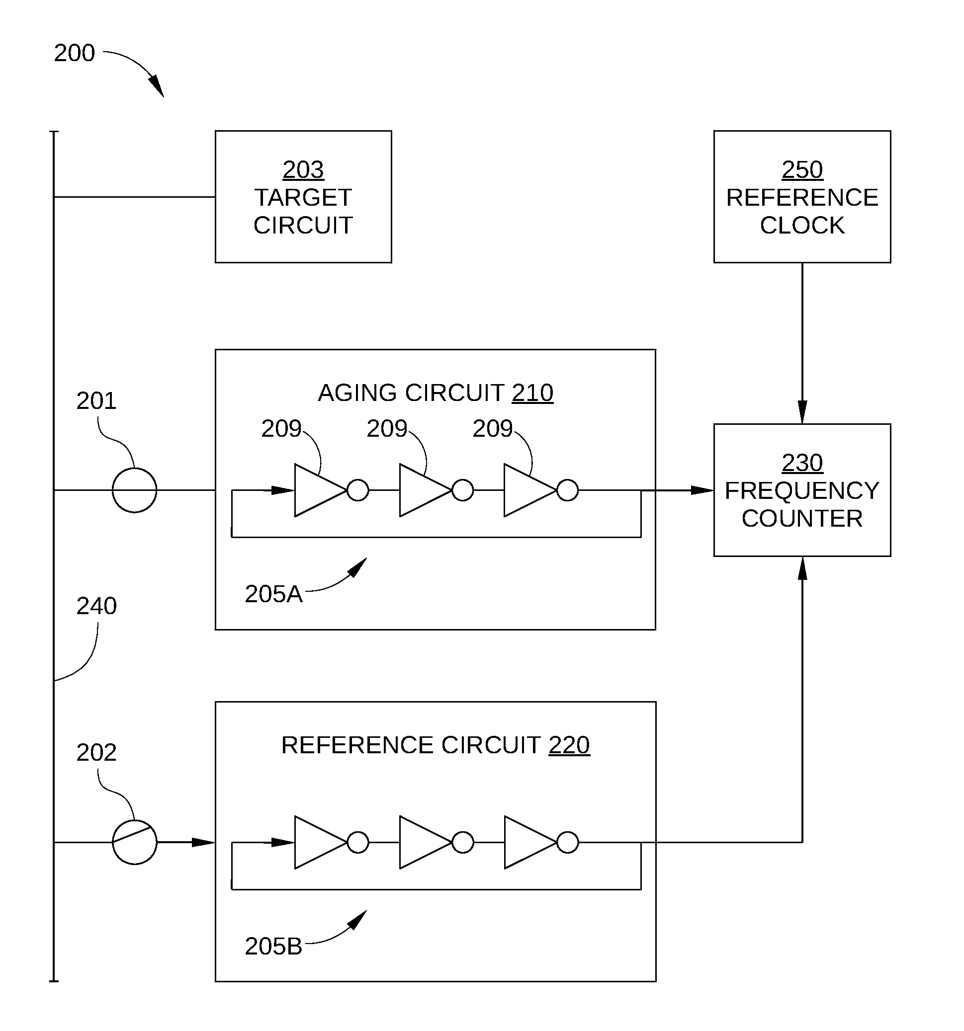
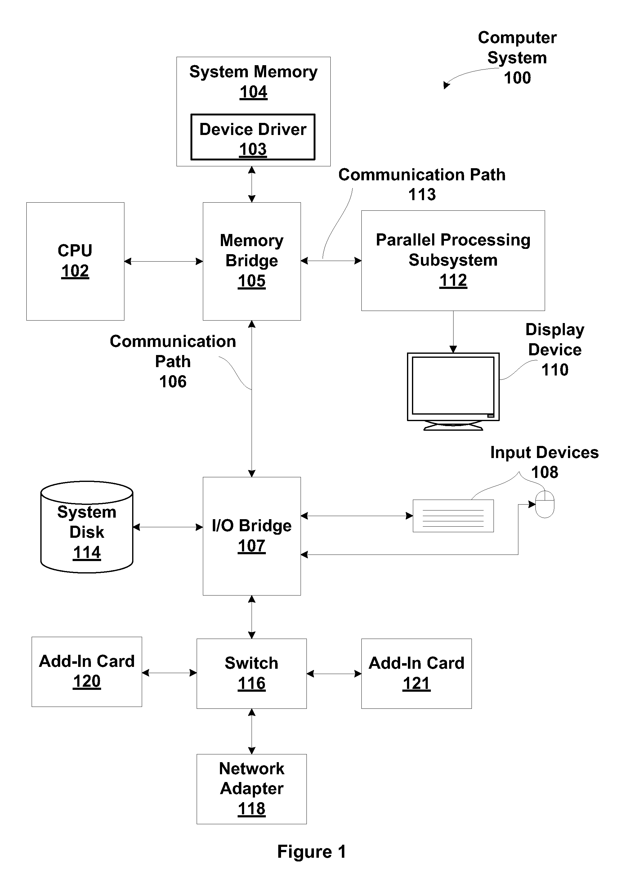
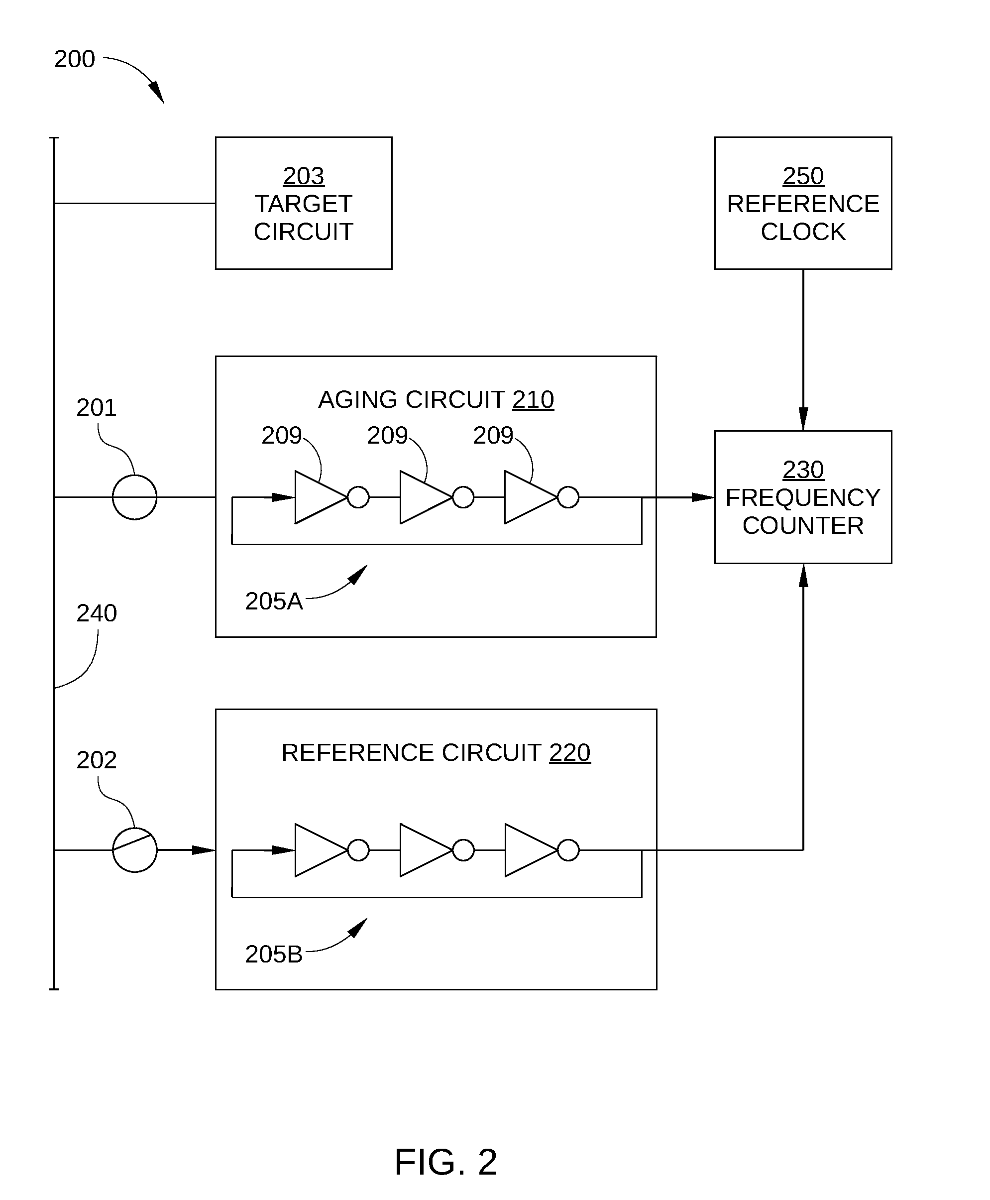
[0018]FIG. 1 is a block diagram illustrating a computer system 100 configured to implement one or more embodiments of the present invention. Computer system 100 includes a central processing unit (CPU) 102 and a system memory 104 communicating via an interconnection path that may include a memory bridge 105. Memory bridge 105, which may be, e.g., a Northbridge chip, is connected via a bus or other communication path 106 (e.g., a HyperTransport link) to an I / O (input / output) bridge 107. I / O bridge 107, which may be, e.g., a Southbridge chip, receives user input from one or more user input devices 108 (e.g., keyboard, mouse) and forwards the input to CPU 102 via communication path 106 and memory bridge 105. A parallel processing subsystem 112 is coupled to memory bridge 105 via a bus or second communication path 113 (e.g., a Peripheral Component Interconnect (PCI) Express, Accelerated Graphics Port, or HyperTransport link). In one embodiment parallel processing subsystem 112 is a grap...


PUM


Abstract

A first instance and a second instance of an oscillating circuit are each formed as part of an integrated circuit and are used to monitor degradation over time of one or more portions of the integrated circuit. The first instance of the oscillating circuit is configured to be coupled to a power source during normal operation of the integrated circuit and the second instance is configured to be decoupled from the power source. Over the lifetime of the integrated circuit, the first instance undergoes degradation from use while the second instance of the oscillating circuit remains unpowered, therefore experiencing essentially no use-related degradation. During a testing operation, the second instance can be used as a reference circuit that accurately quantifies use-related degradation of the first instance of the oscillating circuit and, by extension, one or more portions of the integrated circuit.

Description

BACKGROUND OF THE INVENTION[0001]1. Field of the Invention[0002]Embodiments of the present invention relate generally to integrated circuits and, more specifically, to quantifying silicon degradation in an integrated circuit.[0003]2. Description of the Related Art[0004]In integrated circuits (ICs) and related subsystems, microprocessors and other components can typically be operated across a range of voltages and frequencies. Consequently, a microprocessor or other component of an IC that is operated at a higher frequency (and correspondingly higher voltage) in this range has faster computing performance and higher energy consumption than when operated at a lower frequency (and correspondingly lower voltage). A feature key for saving power and reducing heat generation in ICs is the implementation of dynamic voltage and frequency scaling (DVFS), a combination of dynamic voltage scaling and dynamic frequency scaling. Dynamic voltage scaling is a power management technique in which the...

Claims


Application Information

Patent Timeline
Patent Type & Authority Applications(United States)
IPC IPC(8): G01R23/02H01L25/00
CPCH01L25/00G01R23/02H01L2924/0002G01R31/2858G01R31/2884G06F1/06G06F1/324G06F1/3287G06F1/3296Y02D10/00H01L2924/00H03K3/0315
Inventor KUMAR, HEMANTLONGNECKER, MATTHEW RAYMONDSMITH, BRIAN
Owner NVIDIA CORP
Why Eureka
Try Eureka