
Compound Memory Operations in a Logic Layer of a Stacked Memory

Inactive Publication Date: 2014-06-26
ADVANCED MICRO DEVICES INC
View PDF20 Cites 29 Cited by
  • Summary
  • Abstract
  • Description
  • Claims
  • Application Information

AI Technical Summary

Benefits of technology

This patent discusses a method for improving the performance and efficiency of memory devices. The method involves combining logic and memory layers into a single device, with the logic layer performing various duties such as address generation and control. This helps to reduce the communication of address and control information between the memory and the host processor, improving performance and power efficiency. Additionally, the method allows for greater visibility into memory access patterns, leading to improved scheduling and optimizations. Overall, this approach creates a more efficient and effective memory device.

Problems solved by technology

The transmission of the memory addresses and associated commands consumes power and may introduce performance overheads in cases where the address / command bandwidth becomes a bottleneck.
Furthermore, issuing addresses and control commands on a per-data-item basis may limit opportunities to optimize memory accesses and data transfers.
However, all of these approaches implement address generation on the processor die, and consequently issue a large number of memory access commands and addresses to the memory system, with each access command being directed to an address having a fine level of granularity.

Method used


Image

  • Compound Memory Operations in a Logic Layer of a Stacked Memory
  • Compound Memory Operations in a Logic Layer of a Stacked Memory
  • Compound Memory Operations in a Logic Layer of a Stacked Memory

Examples


Embodiment Construction

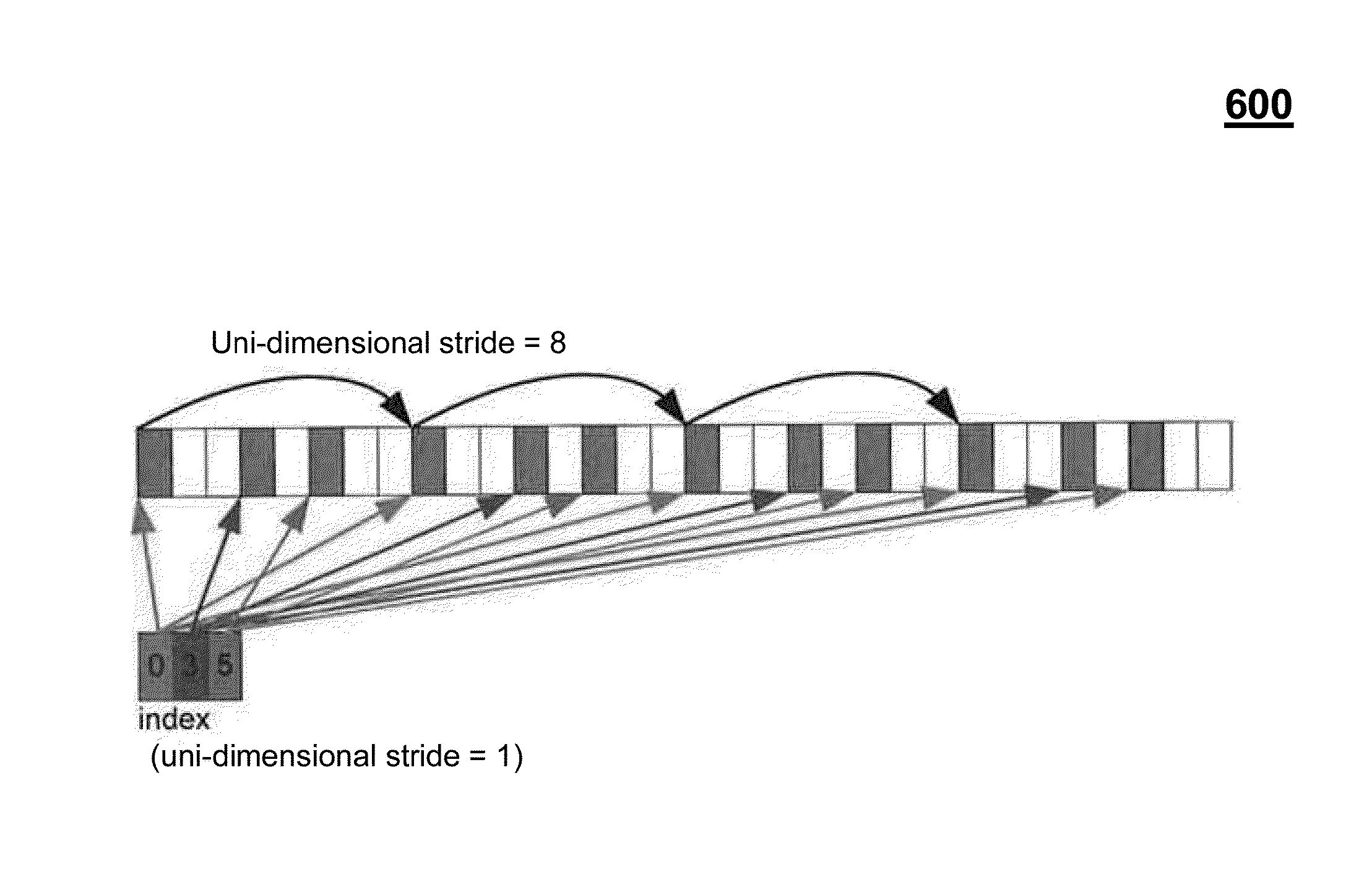
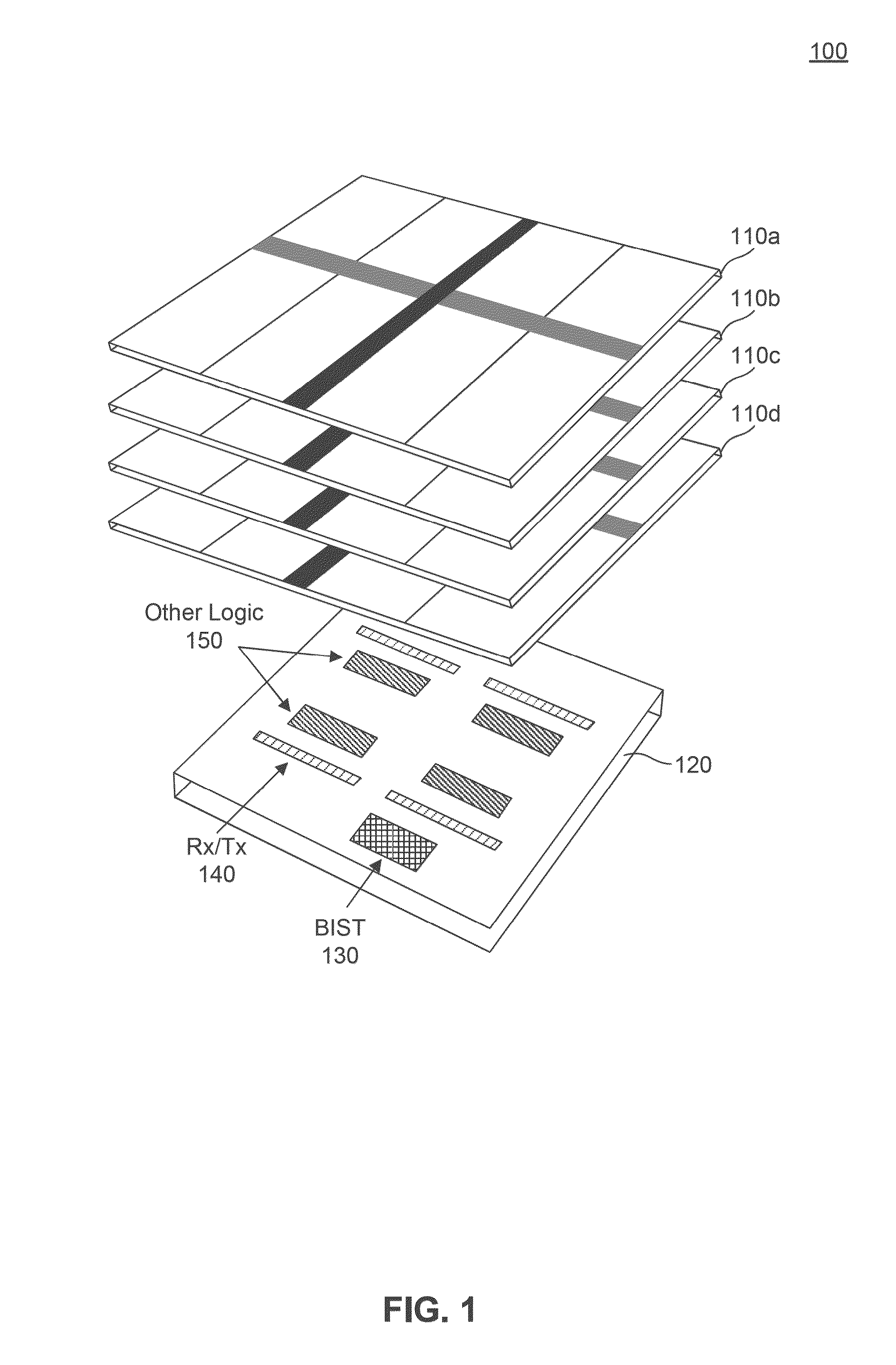
[0008]Some embodiments move address generation and control logic to a logic layer stacked with memory to reduce performance and energy overheads. Some embodiments apply to die-stacked memories that contain a logic layer in addition to one or more layers of DRAM (or other memory technology). This logic layer may be a discrete logic die or logic on a silicon interposer associated with a stack of memory dies. Some embodiments place additional circuitry on the logic layer to implement functionality to perform various data movement and address calculation operations. This functionality enables compound memory operations, i.e., a single request communicated to the memory that characterizes the accesses and movement of many data items. This eliminates the performance and power overheads associated with communicating address and control information on a fine-grain, per-data-item basis from a host processor (or other device) to the memory. This approach also provides better visibility of mac...


PUM


Abstract

Some die-stacked memories will contain a logic layer in addition to one or more layers of DRAM (or other memory technology). This logic layer may be a discrete logic die or logic on a silicon interposer associated with a stack of memory dies. Additional circuitry / functionality is placed on the logic layer to implement functionality to perform various data movement and address calculation operations. This functionality would allow compound memory operations—a single request communicated to the memory that characterizes the accesses and movement of many data items. This eliminates the performance and power overheads associated with communicating address and control information on a fine-grain, per-data-item basis from a host processor (or other device) to the memory. This approach also provides better visibility of macro-level memory access patterns to the memory system and may enable additional optimizations in scheduling memory accesses.

Description

BACKGROUND[0001]1. Field[0002]The disclosed embodiments relate generally to computer systems, and in particular to compound memory operations in memory management.[0003]2. Background Art[0004]Computer systems of various types are ubiquitous in modern society. Common to these computer systems is the storage of data in memory, from which processors perform read, write and other access instructions. A considerable portion of resources in computer systems is employed with the execution of these instructions.[0005]Computer systems typically use processors, where the term “processor” generically refers to anything that accesses memory in a computing system. Processors typically load and store data to / from memory by issuing addresses and control commands on a per-data-item basis. Here a data item may be a byte, a word, a cache line, or the like, as the particular situation requires. These data accesses require a separate address and one or more commands to be transmitted from the processor...

Claims


Application Information

Patent Timeline
IPC IPC(8): G06F12/00
CPCG06F9/3004G06F9/3455G06F15/7821
Inventor JAYASENA, NUWAN S.O'CONNOR, JAMES M.LOH, GABRIEL H.SCHULTE, MICHAEL J.BECKMANN, BRADFORD M.IGNATOWSKI, MICHAEL
Owner ADVANCED MICRO DEVICES INC
Learn More