Metal alloy with an abrupt interface to iii-v semiconductor

a metal alloy and abrupt interface technology, applied in the field of metal alloys with abrupt interfaces, can solve problems such as degrading device performance, and achieve the effects of reducing interface roughness and/or sheet resistance (sheet resistivity), reducing leakage current and/or contact resistance (rc), and reducing interface roughness

Inactive Publication Date: 2014-07-03
SEMATECH
View PDF11 Cites 10 Cited by
  • Summary
  • Abstract
  • Description
  • Claims
  • Application Information

AI Technical Summary

Problems solved by technology

This is particularly true because series resistance degrades device performance by, for example, decreasing drain current.

Method used


Image

  • Metal alloy with an abrupt interface to iii-v semiconductor
  • Metal alloy with an abrupt interface to iii-v semiconductor
  • Metal alloy with an abrupt interface to iii-v semiconductor

Examples


examples b

, C, D, E, and F

[0058]Examples B, C, D, E, and F were prepared using the same process as described in Example A, except different annealing temperatures (250° C., 300° C., 350° C., 450° C., and 500° C., respectively) were used to form the Ni(InP)(InGaAs) alloy.

[0059]Counterexamples B2, C2, D2, E2, and F2.

[0060]Counterexamples B2, C2, D2, E2, and F2 were prepared using the same process as for Counterexample A2, except different annealing temperatures (250° C., 300° C., 350° C., 450° C., and 500° C., respectively) were used to form the Ni—InGaAs alloy.

[0061]FIG. 4 is a plot showing comparative sheet resistivity (Rsheet) values for Examples A-F according to the present invention (fabricated with an InP interlayer) versus Counterexamples A2-F2 (fabricated without an InP interlayer). As is evident from FIG. 4, the metal(III-V) alloys formed with a 5 nm InP layer all had comparable Rsheet values to that of metal(III-V) alloys formed on InGaAs without an InP interlayer. However, at tempera...

examples g

and H

[0062]Examples G and H were prepared using the same process as described in Example A, except that 10 nm and 15 nm of Ni, respectively for Example G and Example H, were deposited instead of 5 nm of Ni.

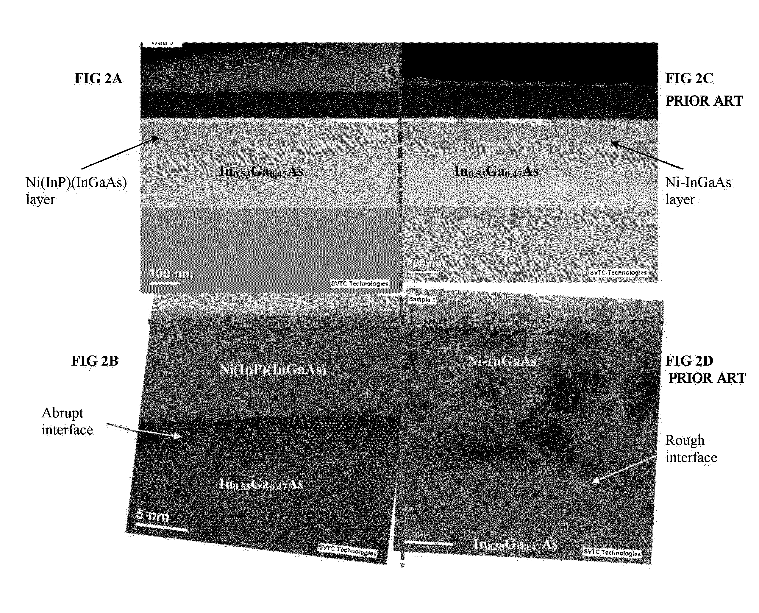
[0063]FIGS. 5A-D are XTEM micrograph images of metal / III-V interfaces in semiconductor structures. FIG. 5A corresponds to the semiconductor structure of Example A, whereas FIGS. 5B and 5C correspond to Example G and Example H, respectively. FIG. 5D is an image of a portion of the semiconductor structure fabricated in Counterexample A2. FIGS. 5A-C demonstrate that the metal / III-V interface remained smooth even at a metal(InP)(III-V) alloy thickness of 28 nm, which is considerably thicker than the 5 nm InP interlayer thickness. FIG. 5D demonstrates that even at a Ni thickness of 5 nm, the metal / III-V interface of the semiconductor structure fabricated without an InP layer is non-planar with significant variations in the alloy thickness (14-23 nm).


PUM

PropertyMeasurementUnit
thickaaaaaaaaaa
thickaaaaaaaaaa
temperatureaaaaaaaaaa

Abstract

Semiconductor structures having a first layer including an n-type III-V semiconductor material and a second layer including an M(InP)(InGaAs) alloy, wherein M is selected from Ni, Pt, Pd, Co, Ti, Zr, Y, Mo, Ru, Ir, Sb, In, Dy, Tb, Er, Yb, and Te, and combinations thereof, are disclosed. The semiconductor structures have a substantially planar interface between the first and second layers. Methods of fabricating semiconductor structures, and methods of reducing interface roughness and / or sheet resistance of a contact are also disclosed.

Description

TECHNICAL FIELD[0001]The invention relates to semiconductor structures, to methods of fabricating semiconductor structures, and to methods of reducing interface roughness and / or sheet resistance (sheet resistivity) of a contact at elevated temperatures.BACKGROUND OF THE INVENTION[0002]The use of III-V compound semiconductors has been widely explored as a means to improve integrated circuit performance.[0003]Various metal layers have been used as semiconductor device contacts due to their good electrical properties and relatively high thermal stability. For example, a Ni—InGaAs source / drain contact scheme for III-V metal-oxide-semiconductor field effect transistors (MOSFET) has been developed. The Ni—InGaAs layer may be formed, for example, onto an exposed surface of source and drain regions in a semiconductor substrate. During an annealing process, atoms of the substrate in the source and drain regions react with the atoms of the deposited metal, thereby forming a layer. Portions of...

Claims


Application Information

Patent Timeline
Patent Type & Authority Applications(United States)
IPC IPC(8): H01L29/205
CPCH01L29/205H01L21/28575H01L29/452H01L29/4966H01L29/513H01L29/517H01L29/66522
Inventor LEE, RINUS TEK POKIM, TAE WOOWONG, MAN HOIHILL, RICHARD
Owner SEMATECH
Why Eureka
Try Eureka