Equipment for manufacturing semiconductor

a technology for semiconductors and equipment, applied in the direction of crystal growth process, polycrystalline material growth, chemically reactive gases, etc., can solve the problems of high temperature unsuitable for manufacturing process, substrate deterioration with respect to etching, and the selective epitaxy process has several limitations

Inactive Publication Date: 2014-07-10
EUGENE TECH CO LTD
View PDF4 Cites 175 Cited by
  • Summary
  • Abstract
  • Description
  • Claims
  • Application Information

AI Technical Summary

Benefits of technology

[0006]The present invention also provides an equipment for manufacturing a semiconductor which can r...

Problems solved by technology

Generally, the selective epitaxy process has several limitations.
Also, features of the substrate may be deteriorated with respect to the etching.
Here...

Method used


Image

  • Equipment for manufacturing semiconductor
  • Equipment for manufacturing semiconductor
  • Equipment for manufacturing semiconductor

Examples


Embodiment Construction

[0028]Hereinafter, exemplary embodiments of the present invention will be described in detail with reference to FIGS. 1 to 9. The present invention may, however, be embodied in different forms and should not be constructed as limited to the embodiments set forth herein. Rather, these embodiments are provided so that this disclosure will be thorough and complete, and will fully convey the scope of the present invention to those skilled in the art. In the drawings, the shapes of components are exaggerated for clarity of illustration.

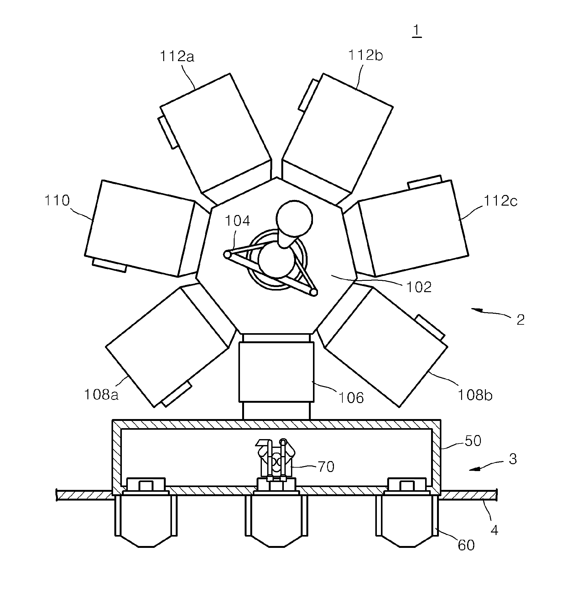
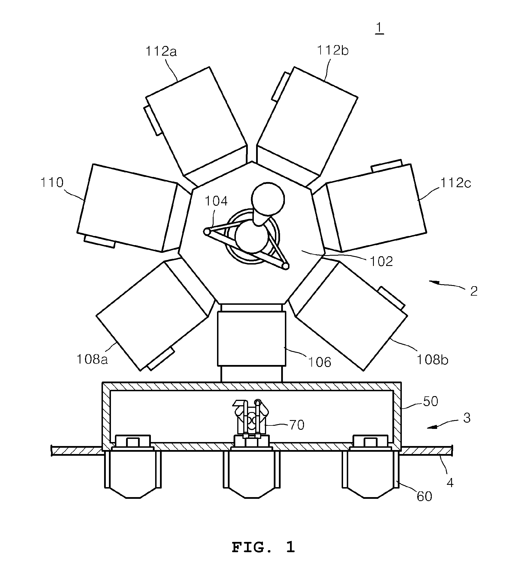
[0029]FIG. 1 is a schematic view of an equipment 1 for manufacturing a semiconductor according to an embodiment of the present invention. The equipment 1 for manufacturing the semiconductor includes a process equipment 2, an equipment front end module (EFEM) 3, and an interface wall 4. The EFEM 3 is mounted on a front side of the process equipment 2 to transfer a wafer W between a container (not shown) in which substrates S are received and the process equ...


PUM

PropertyMeasurementUnit
Vacuumaaaaaaaaaa

Abstract

Provided is an equipment for manufacturing a semiconductor. The equipment for manufacturing a semiconductor includes a cleaning chamber in which a cleaning process is performed on substrates, an epitaxial chamber in which an epitaxial process for forming an epitaxial layer on each of the substrates is performed, and a transfer chamber to which the cleaning chamber and the epitaxial chamber are connected to sides surfaces thereof, the transfer chamber including a substrate handler for transferring the substrates, on which the cleaning process is completed, into the epitaxial chamber.

Description

CROSS-REFERENCE TO RELATED APPLICATIONS[0001]This U.S. non-provisional patent application claims priority under 35 U.S.C. §119 of Korean Patent Application No. 10-2011-0077100, filed on Aug. 2, 2011, the entire contents of which are hereby incorporated by reference.BACKGROUND OF THE INVENTION[0002]The present invention disclosed herein relates to an equipment for manufacturing a semiconductor, and more particularly, to an equipment for manufacturing a semiconductor which performs an epitaxial process for forming an epitaxial layer on a substrate.[0003]Typical selective epitaxy processes involve deposition and etching reactions. The deposition and etching reactions may occur simultaneously at slightly different reaction rates with respect to a polycrystalline layer and an epitaxial layer. While an existing polycrystalline layer and / or an amorphous layer are / is deposited on at least one second layer during the deposition process, the epitaxial layer is formed on a single crystal surfa...

Claims


Application Information

Patent Timeline
IPC IPC(8): C30B25/10
CPCC30B25/10H01L21/67178H01L21/67207H01L21/67757H01L21/02046C30B25/08C30B29/06C30B35/00
Inventor KIMHYON, JUN JINWOO, SANG HOSHIN, SEUNG WOOKIM, HAI WON
Owner EUGENE TECH CO LTD
Why Eureka
Try Eureka