RF ldmos device and method of forming the same

Active Publication Date: 2014-07-10
SHANGHAI HUAHONG GRACE SEMICON MFG CORP
View PDF1 Cites 7 Cited by
  • Summary
  • Abstract
  • Description
  • Claims
  • Application Information

AI Technical Summary

Benefits of technology

[0019]Firstly, the first well can form a low-resistance channel under the channel doped region, which is capable of effectively reducing the total channel resistance and inhibiting the occurrence of snapback effect, while not affecting other characteristics of the RF LDMOS device.
[0020]Secondly, dopant ions can laterally diffuse from the first well into an area under a first end of the drift region, resulting in improvement of electric field uniformity in the drift region. Moreover, the dopant ions can further create a Reduced SURfsce Field (RESURF) effect in

Problems solved by technology

With this design, in the event of a high voltage applied on the drain region 9, a snapback

Method used


Image

  • RF ldmos device and method of forming the same
  • RF ldmos device and method of forming the same
  • RF ldmos device and method of forming the same

Examples


Embodiment Construction

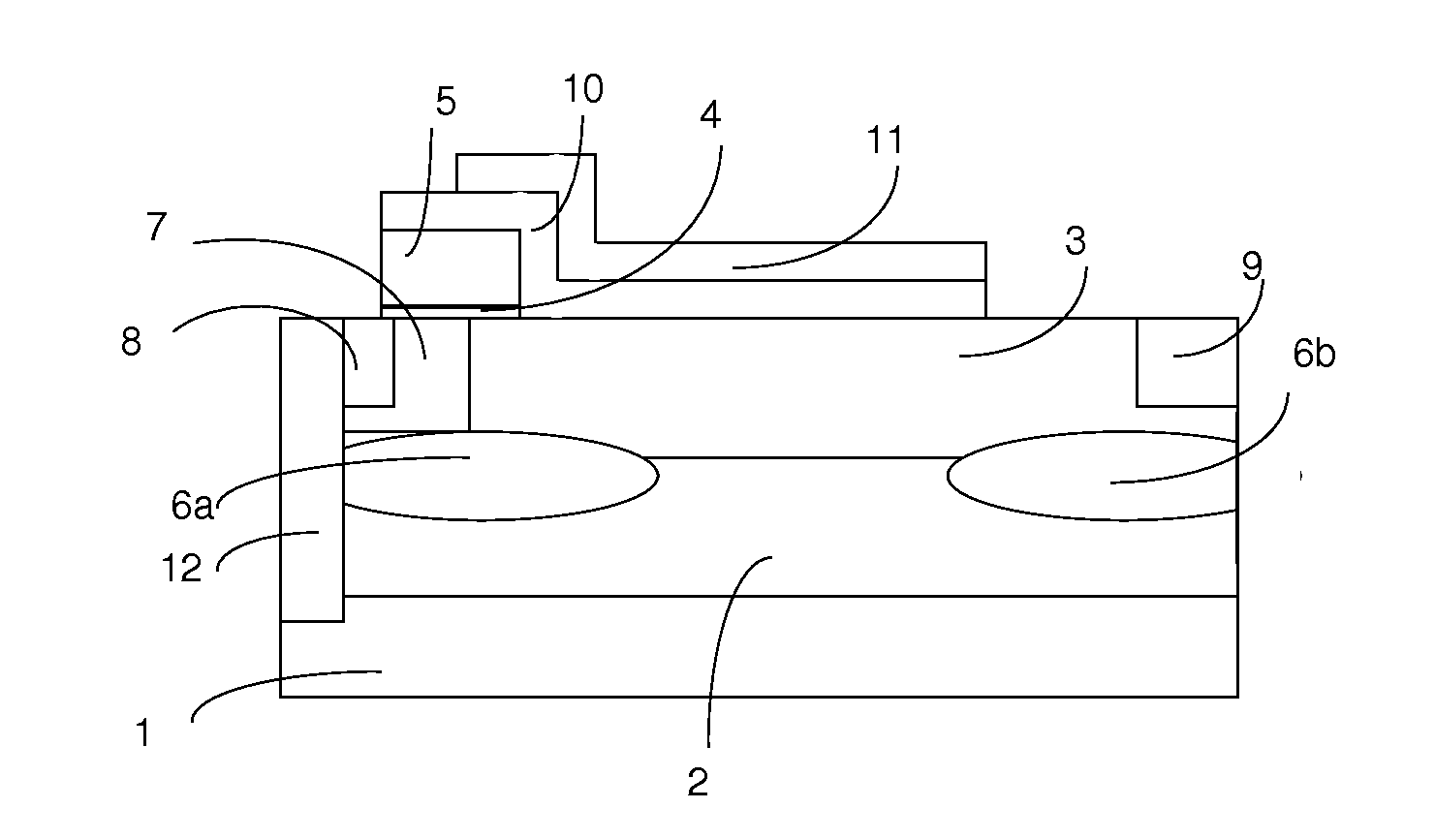
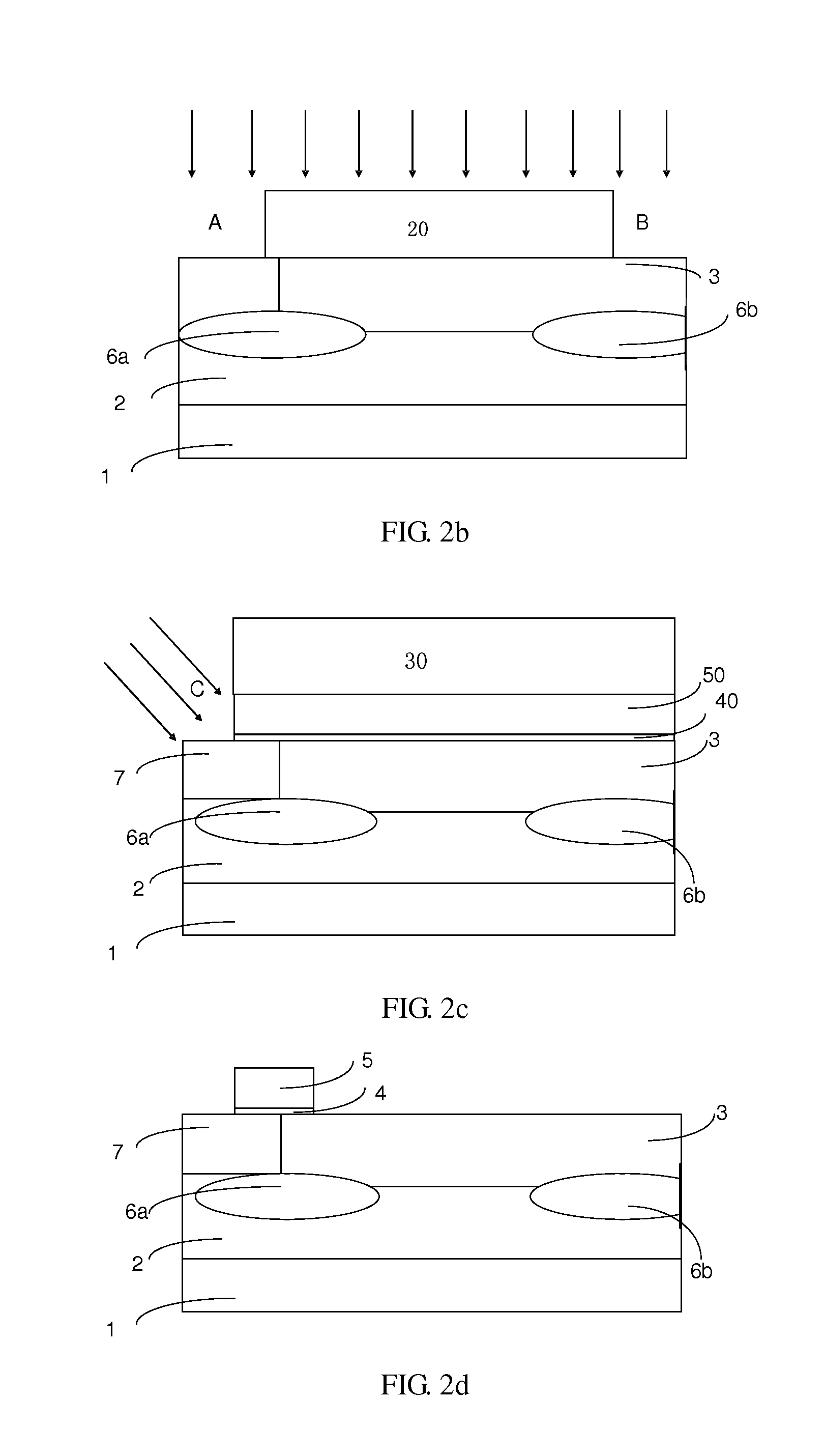
[0024]FIG. 2h is a schematic illustration of a radio frequency (RF) laterally diffused metal oxide semiconductor (LDMOS) device constructed in accordance with the present invention, which may be either a p-channel device or an n-channel device. In some embodiments, as illustrate in FIG. 2h, the RF LDMOS device is an N-channel device including a heavily-doped p-type substrate 1 and a lightly-doped p-type epitaxial layer 2 formed on the substrate 1. In the epitaxial layer 2, there are formed: a p-type channel region 7 and an n-type drift region 3, in contact with each other side by side; and a first p-type well 6a and a second p-type well 6b, independent from each other. The first well 6a underlies and contacts both of the channel region 7 and the drift region 3 at where the two regions come in contact. The second well 6b is under and in contact with an end of the drift region 3 away from the channel region 7. A heavily-doped n-type region acting as a source region 8 is formed in the ...


PUM


Abstract

An RF LDMOS device is disclosed, including: a substrate having a first conductivity type; a channel doped region having the first conductivity type and a drift region having a second conductivity type, each in an upper portion of the substrate, the channel doped region having a first end in lateral contact with a first end of the drift region; a first well having the first conductivity type in the substrate, the first well having a top portion in contact with both of a bottom of the first end of the channel doped region and a bottom of the first end of the drift region; and a second well having the first conductivity type in the substrate, the second well having a top portion in contact with a bottom of a second end of the drift region. A method of forming such an RF LDMOS device is also disclosed.

Description

CROSS-REFERENCE TO RELATED APPLICATION[0001]This application claims the priority of Chinese patent application number 201310003606.6, filed on Jan. 6, 2013, the entire contents of which are incorporated herein by reference.TECHNICAL FIELD[0002]The present invention relates generally to semiconductor devices, and in particular, to a laterally diffused metal oxide semiconductor (LDMOS) device usable in radio frequency (RF) applications.BACKGROUND[0003]RF LDMOS devices are commonly used in high-power RF applications, such as RF base stations and RF broadcast stations. In general, RF LDMOS devices are used in plurality to form an array, in which each device is required to have substantial reliability in operation to avoid the whole array becoming useless upon unexpected failure (e.g., premature breakdown) of any susceptible RF LDMOS device.[0004]FIG. 1 shows an existing RF LDMOS device, which can be either a P-channel or N-channel one. In the case of an N-channel RF LDMOS device, as ill...

Claims


Application Information

Patent Timeline
IPC IPC(8): H01L29/78H01L21/265H01L29/66
CPCH01L29/7816H01L29/66681H01L21/265H01L21/26586H01L29/063H01L29/0634H01L29/1033H01L29/1083H01L29/402H01L29/66659H01L29/7835
Inventor QIAN, WENSHENG
Owner SHANGHAI HUAHONG GRACE SEMICON MFG CORP
Why Eureka
Try Eureka