Electric field emitting source, element using same, and production method therefor

a field emission source and field emission technology, applied in the manufacture of discharge tubes/lamps, discharge tube main electrodes, electrode systems, etc., can solve the problems of difficult to ensure the uniformity of catalyst metal deposition on a large area, difficult to control the size of catalyst metal particles, and low adhesion between the grown nano-material and the cathode substrate, so as to achieve the effect of reducing the entire production process

Active Publication Date: 2014-07-10
LUMINAX CO LTD
View PDF8 Cites 16 Cited by
  • Summary
  • Abstract
  • Description
  • Claims
  • Application Information

AI Technical Summary

Benefits of technology

[0033]According to the present disclosure, it is possible to obtain a field emission source, which can very firmly fix an electron emission structure, and an electron emission device using the same. This is achieved by producing an electron emission unit in a film form and fixing an end of the electron emission film by means of a first block and a second block of a cathode. According to the present disclosure, it is possible to obtain a field emission source and an electron emission device, which can realize a horizontal electron emission structure without requiring a spacer. Since the spacer that has been necessary in a conventional vertical structure is excluded, a process for forming the spacer can be omitted. Especially, since the whole structure is formed on one substrate, the entire production process can be reduced, compared to a conventional production process. In addition, since the structure is formed on one substrate, it is possible to obtain an integrated array structure of multiple field electron emission devices. If necessary, it is possible to produce a large number of individual field emission devices by separating the array into individual device units. As the field electron emission devices having the above-described structure, for example, there are lamps, display devices, backlight devices for flat panel displays and electron sources for high power microwaves. In addition, since independent driving of a selective individual device is possible, and connection between individual devices is possible, an integrated vacuum electron emission device in the similar form to that of a solid semiconductor device can be realized.

Problems solved by technology

The directly growing method enables easy control of a structure of the nano-material such as control of a diameter, length, density and patterning, but is disadvantageous in that it is difficult to assure uniformity of catalyst metal deposition on a large area and control a size of catalyst metal particles, and adhesion between the grown nano-material and the cathode substrate is low.
However, the screen printing method is disadvantageous in that it is difficult to control density of an active electron emission cite, the field electron emission characteristic is easily deteriorated due to various organic / inorganic binders and polymers, and processes are complicated.
However, since controlling thickness and density is difficult, uniformity and reproducibility are poor, and adhesion to the cathode substrate is low, there is a problem in reliability and stability when the electrophoresis is applied to field electron emission.
However, like the electrophoresis, the self-assembling method is disadvantageous in that the adhesion between the formed nano-material thin film and the cathode substrate is poor, and much time is needed.
However, since the thin film surface state is determined depending on a degree of evaporation of a suspension during movement of a spray droplet from a nozzle to the cathode substrate, control of thickness and density of a nano-material thin film and uniform deposition of a thin film are difficult.
Accordingly, uniformity and reproducibility are deteriorated.
However, the inkjet printing method is disadvantageous in that the adhesion between the printed nano-material and the cathode substrate is low.

Method used


Image

  • Electric field emitting source, element using same, and production method therefor
  • Electric field emitting source, element using same, and production method therefor
  • Electric field emitting source, element using same, and production method therefor

Examples


Embodiment Construction

[0040]Hereinafter, a fundamental structure of a field emission source in accordance with illustrative embodiments of the present disclosure will be described with reference to the accompanying drawings.

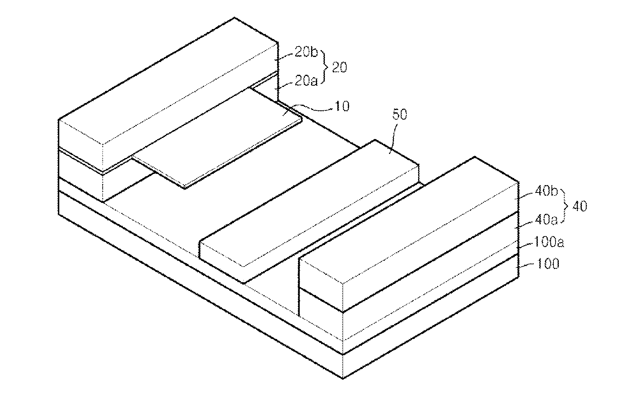
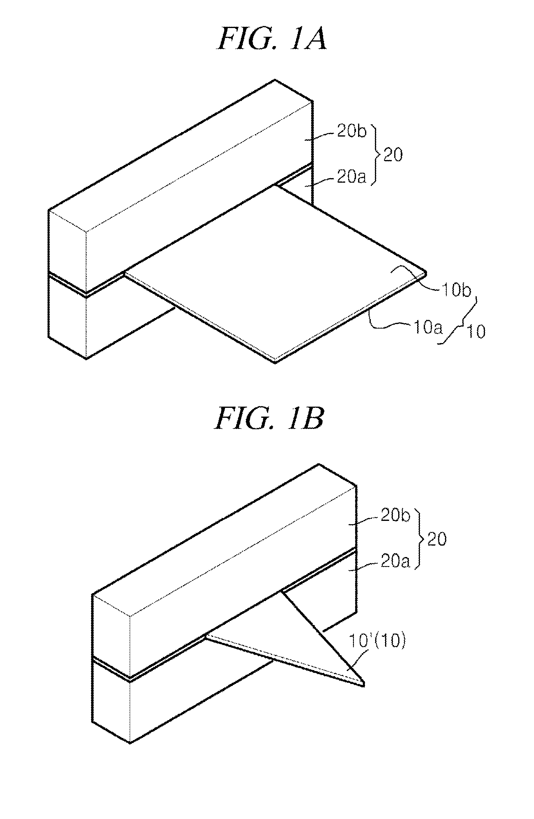
[0041]First, with reference to FIG. 1a, an electron emission film 10, which can be in various forms, is fixed to a cathode 20. In this case, the cathode 20 has a first block 20a and a second block 20b. One end of the electron emission film 10 is inserted between the first and second blocks 20a and 20b. The electron emission film 10 has a first surface 10a (the bottom surface in the drawing) and a second surface 10b (the top surface in the drawing) opposite to the first surface 10a. The first surface 10a of the electron emission film 10 is facing to the top surface of the first block 20a, and the second surface 10b of the electron emission film 10 is facing to the bottom surface of the second block 20b. In view of structure, since a certain width of one end of the electron emission fil...


PUM


Abstract

An electric field emitting source is equipped with an electron emitting film which comprises a nano-sized electron emitting substance and has a first surface and a second surface constituting the surface opposite thereto, and a cathode which secures one end of the electron emitting film and comprises a first block and a second block respectively corresponding to the first surface and the second surface of the electron emitting film.

Description

CROSS-REFERENCE TO RELATED APPLICATION[0001]This application claims the benefit of Korean Patent Application No. 10-2011-0068553 filed on Jul. 11, 2011 and PCT Patent Application No. PCT / KR2012 / 005480 filed on Jul. 11, 2012, the entire disclosures of which are incorporated herein by reference.FIELD OF THE INVENTION[0002]The present disclosure relates to a field emission source and a field emission device, in particular, a field emission device using a nano-material film and a production method thereof.BACKGROUND OF THE INVENTION[0003]Conventional methods for producing a field emission source by using a nano-sized electron emission material (hereinafter, referred to as “nano-material”) in a particle or rod form can be divided into a method for growing a nano-material directly on a cathode substrate [(Science vol. 283, 512, 1999), (Chemical Physics Letters. 312, 461, 1999), (Chemical Physics Letters. 326, 175, 2000), (Nano Letter vol. 5, 2153, 2005), US006350488B1, US006514113B1], and...

Claims


Application Information

Patent Timeline
Patent Type & Authority Applications(United States)
IPC IPC(8): H01J19/24H01J9/02
CPCH01J19/24H01J9/025H01J1/304H01J3/021H01J1/30H01J9/02
Inventor LEE, CHEOL JINSHIN, DONG HOONSHIN, JI HONG
Owner LUMINAX CO LTD
Why Eureka
Try Eureka