Wafer packaging method

a packaging method and wafer technology, applied in the direction of electrical equipment, semiconductor devices, radio frequency controlled devices, etc., can solve the problems of difficulty in manufacturing process, more likely mechanical strength of thin glass, etc., and achieve the effect of easy alignment, increased strength of light transmissive protection sheets and wafers, and easy separation

Active Publication Date: 2014-07-31
XINTEC INC
View PDF3 Cites 0 Cited by
  • Summary
  • Abstract
  • Description
  • Claims
  • Application Information

AI Technical Summary

Benefits of technology

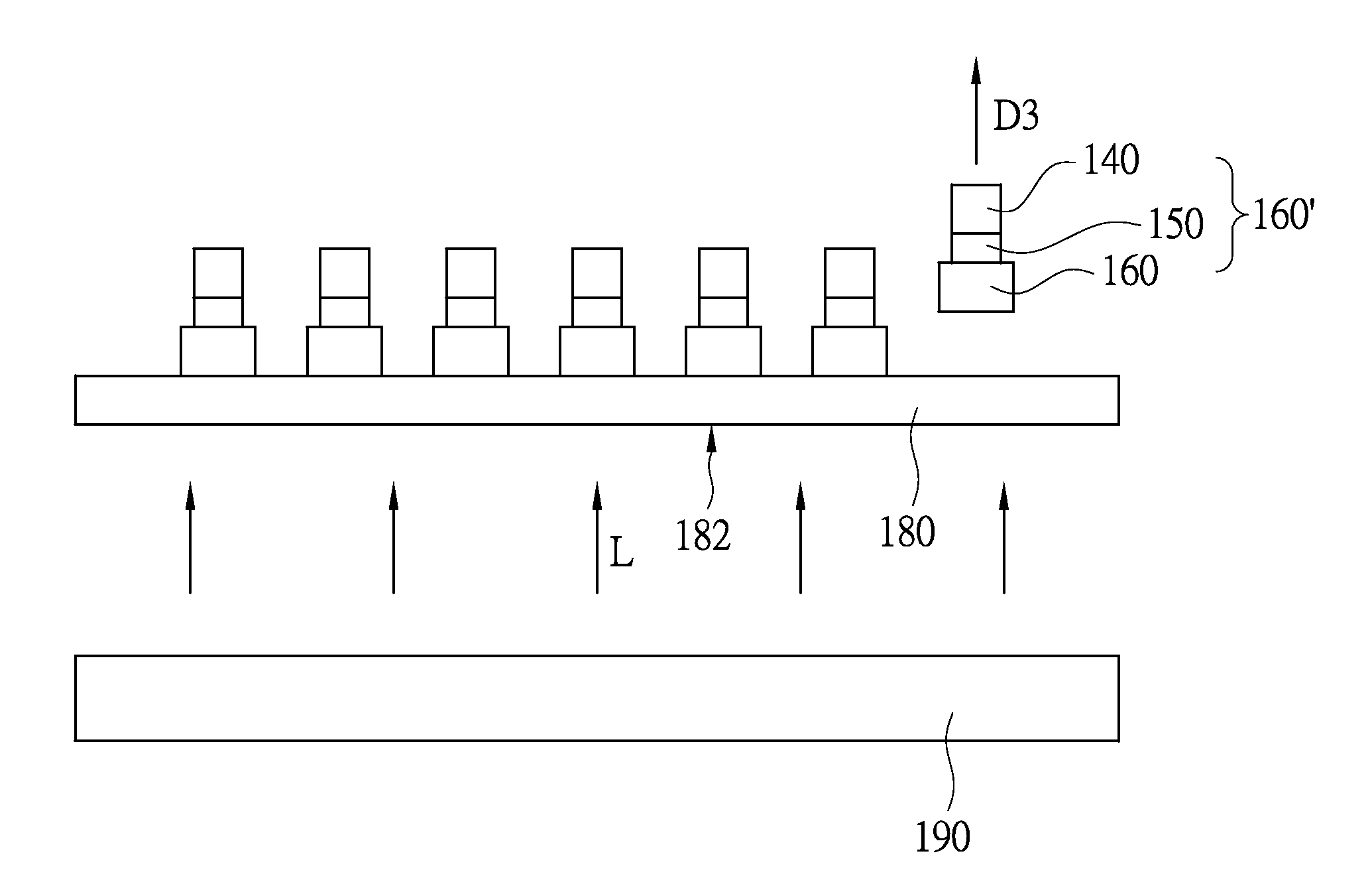
[0023]In the aforementioned embodiments of the present invention, the hydrolytic temporary bonding layer is utilized to adhere the light transmissive protection sheet and the light transmissive carrier in the wafer packaging method. The strength of the light transmissive carrier is sufficient to prevent the light transmissive protection sheet from warpage when the light transmissive protection sheet is adhered to the wafer. As a result, since when the light transmissive protection sheet is adhered to the wafer, the warpage of the light transmissive protection sheet is not easily happened, and the light transmissive carrier can be attached by static electricity and has transmittance, the light transmissive protection sheet can be easily aligned with the wafer and does not shift on the wafer. When the wafer is ground, the strength of the light transmissive protection sheet and the wafer is increased by the light transmissive carrier, such that the light transmissive protection sheet and the wafer are not easily broken. In addition, the adhesion force of the hydrolytic temporary bonding layer is eliminated in high temperature liquid. Therefore, after the wafer is ground, the light transmissive carrier can be easily separated from the light transmissive protection sheet.
[0024]Since the strength of the light transmissive protection sheet and the wafer can be increased by the light transmissive carrier, the tape adhering process in the prior art can be omitted. The wafer packaging method can use a significantly thin light transmissive protection sheet to improve the transmittance thereof, such that the image detecting ability of chips formed by the diced wafer can be improved. Moreover, when the wafer is ground, the ground thickness of the wafer can be flexibly adjusted.

Problems solved by technology

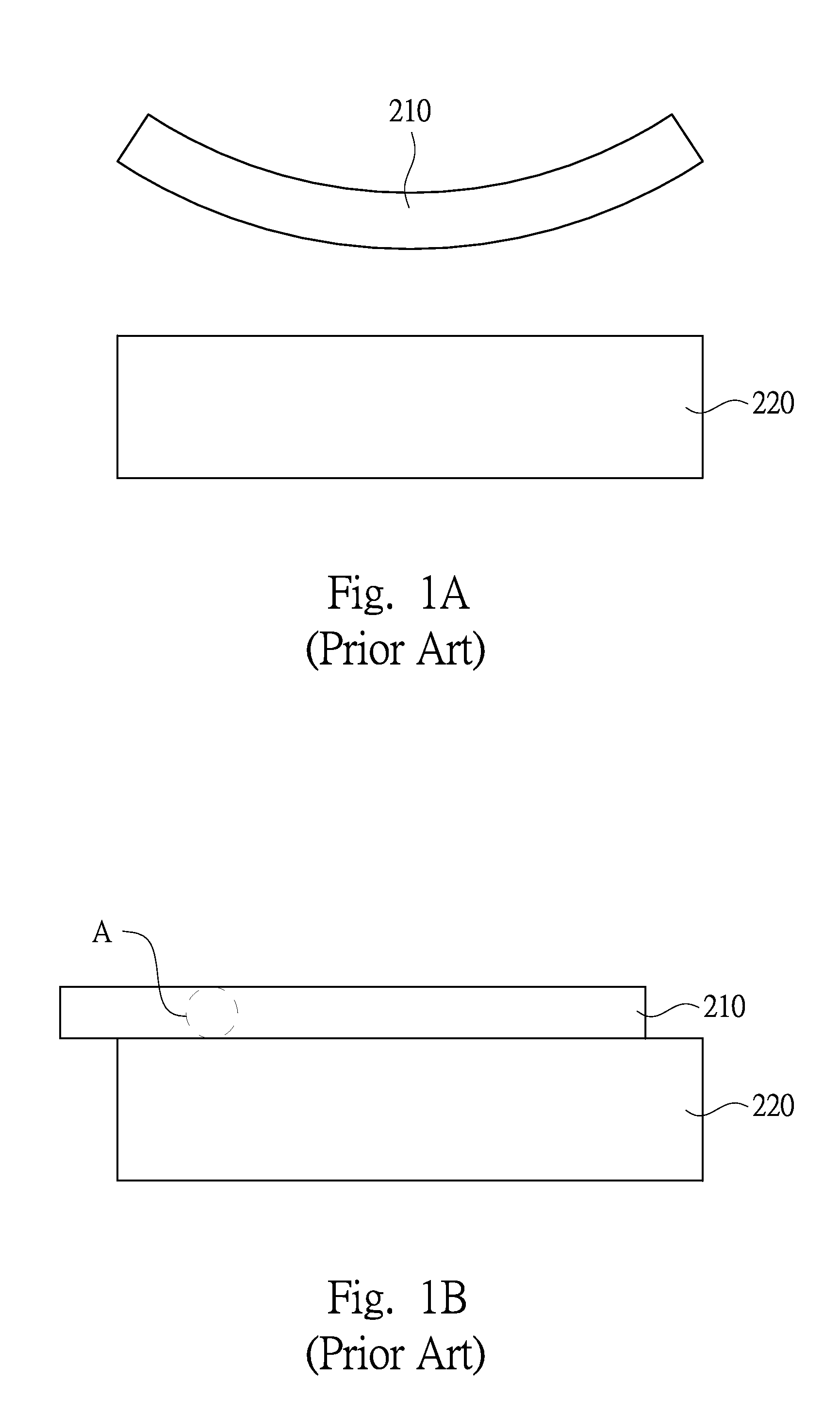
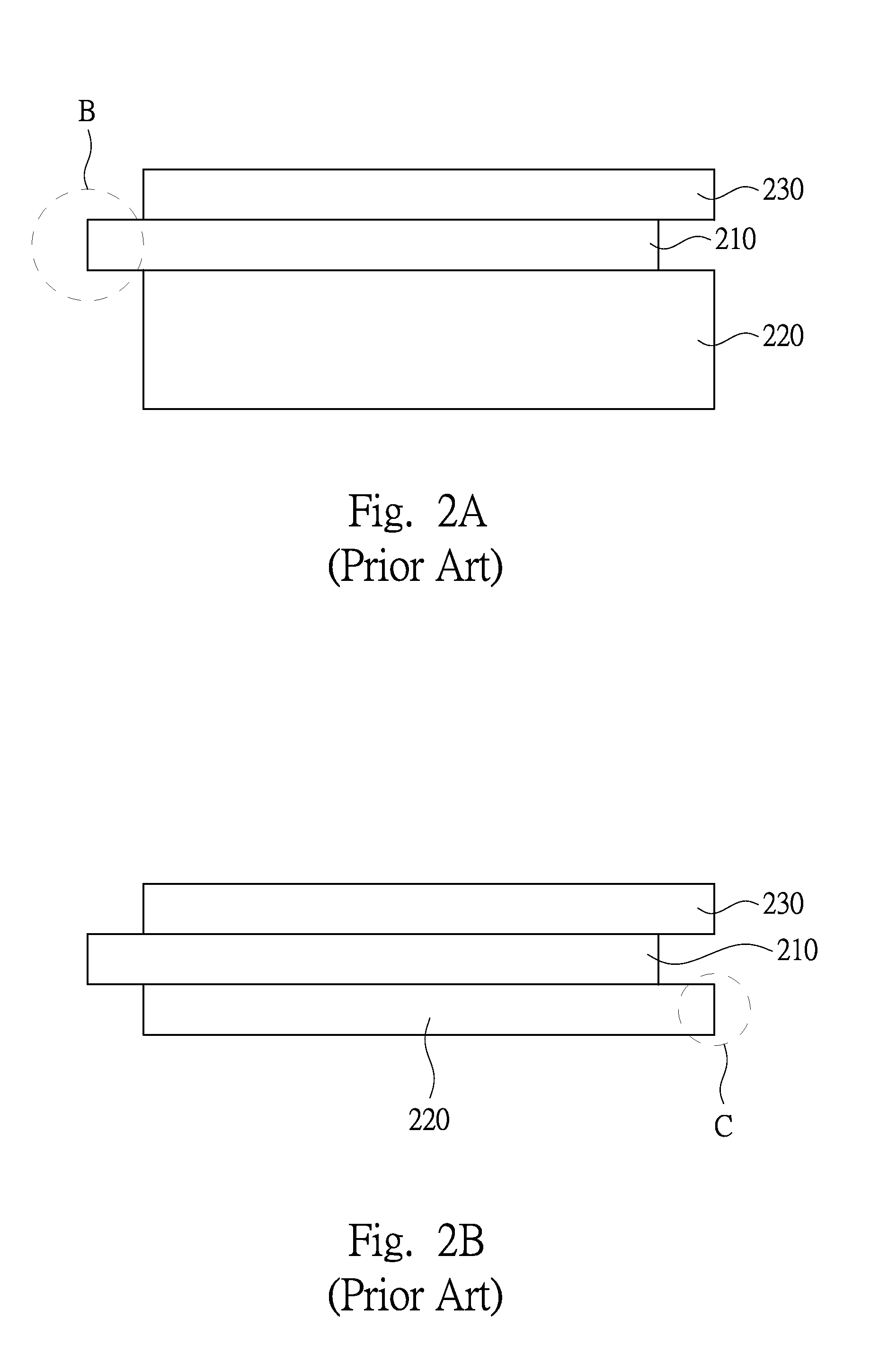
Although a thinner glass sheet can provide a better light transmittance and improved image detecting ability of chips formed from the diced wafer, the strength of the thin glass is more likely of lacking mechanical strength and having warpage, so as to increase the difficulty in the manufacturing process of the wafer.

Method used


Image

  • Wafer packaging method
  • Wafer packaging method
  • Wafer packaging method

Examples


Embodiment Construction

[0048]Reference will now be made in detail to the present embodiments of the invention, examples of which are illustrated in the accompanying drawings. Wherever possible, the same reference numbers are used in the drawings and the description to refer to the same or like parts.

[0049]FIG. 3 is a flow chart of a wafer packaging method according to one embodiment of the present invention. In step S1, a light transmissive carrier is provided. Thereafter in step S2, a hydrolytic temporary bonding layer is formed on the light transmissive carrier. Next in step S3, a first surface of a light transmissive protection sheet is bonded to the hydrolytic temporary bonding layer, such that the hydrolytic temporary bonding layer is located between the light transmissive protection sheet and the light transmissive carrier. Thereafter in step S4, a second surface of the light transmissive protection sheet facing away from the first surface is bonded to a third surface of a wafer, and the third surfa...


PUM


Abstract

A wafer packaging method includes the following steps. A light transmissive carrier is provided. A hydrolytic temporary bonding layer is formed on the light transmissive carrier. A first surface of a light transmissive protection sheet is bonded to the hydrolytic temporary bonding layer, such that the hydrolytic temporary bonding layer is located between the light transmissive protection sheet and the light transmissive carrier. A second surface of the light transmissive protection sheet facing away from the first surface is bonded to a third surface of a wafer. The light transmissive carrier, the hydrolytic temporary bonding layer, the light transmissive protection sheet, and the wafer are immersed in a high temperature liquid, such that adhesion force of the hydrolytic temporary bonding layer is eliminated. The light transmissive protection sheet and the wafer are obtained from the high temperature liquid.

Description

RELATED APPLICATIONS[0001]This application claims priority to U.S. provisional Application Ser. No. 61 / 758,417, filed Jan. 30, 2013, which is herein incorporated by reference.BACKGROUND[0002]1. Field of Invention[0003]The present invention relates to a wafer packaging method.[0004]2. Description of Related Art[0005]With the advance in glass cutting technology, glass manufacturers are able to manufacture glass sheets with thickness under 400 μm. When an image sensor wafer, e.g., a CMOS wafer, is packaged, a glass sheet is needed to cover the surface of the wafer for the wafer protection. Although a thinner glass sheet can provide a better light transmittance and improved image detecting ability of chips formed from the diced wafer, the strength of the thin glass is more likely of lacking mechanical strength and having warpage, so as to increase the difficulty in the manufacturing process of the wafer.[0006]FIG. 1A is a schematic view of a glass sheet 210 when being adhered to a wafer...

Claims


Application Information

Patent Timeline
Patent Type & Authority Applications(United States)
IPC IPC(8): H01L27/146
CPCH01L27/14687H01L27/14618H01L2924/0002H01L2924/00H01L21/2007
Inventor CHEN, CHIH-HAOLOU, BAI-YAOCHEN, SHIH-KUANG
Owner XINTEC INC
Why Eureka
Try Eureka