Thin film solar cell and manufacturing method therefor

a solar cell and film technology, applied in the field can solve the problems of insufficient art of forming such an insulation film, insufficient photovoltaic conversion efficiency of crystal-type solar cells, and insufficient so as to and improve the photovoltaic conversion efficiency of thin film solar cells

Active Publication Date: 2014-08-07
SOLAR FRONTIER
View PDF1 Cites 10 Cited by
  • Summary
  • Abstract
  • Description
  • Claims
  • Application Information

AI Technical Summary

Benefits of technology

[0009]Therefore, an object of the present invention is to realize a thin film solar cell which is provided with easily formed point contact between the light absorption layer and the electrode layer.
[0020]According to the present invention, the interface between the metal back surface electrode layer and the p-type light absorption layer is formed with a nanoparticle dispersed layer which includes nanoparticles with surfaces comprised of insulators. Due to this, the contact area between the metal back surface electrode layer and the p-type light absorption layer is greatly limited and point contact can be realized. Due to this point contact, the recombination speed of the carriers at the interface between the metal back surface electrode layer and the p-type light absorption layer greatly falls and the carriers which are produced by the incident light efficiently reach the electrodes without being recombined, so the thin film solar cell is improved in photovoltaic conversion efficiency. Furthermore, when the insulators of the surfaces of nanoparticles have a refractive index which is smaller than the refractive index of the light absorption layer, the nanoparticles are made a particle size of 100 nm or more to enable the nanoparticle dispersed layer to function as a BSR (back surface reflector) structure and further improve the thin film solar cell in photovoltaic conversion efficiency.
[0021]Further, for example, when using nanoparticles which are comprised of gold (Au) or silver (Ag) particles which are covered by an insulation film so as to form the nanoparticle dispersed layer, the nanoparticles are made a particle size of 100 nm or less to enable surface plasmon resonance at the nanoparticle dispersed layer and further improve the thin film solar cell in photovoltaic conversion efficiency.
[0022]The nanoparticle dispersed layer can be easily formed by coating and drying a solution which contains the nanoparticles on the metal back surface electrode layer or light absorption layer. Therefore, according to the present invention, it is possible to easily realize point contact at the thin film solar cell.

Problems solved by technology

On the other hand, in general, their photovoltaic conversion efficiency is inferior to that of crystal-type solar cell.
However, in current thin film solar cells, the above such point contact structure is not realized.
When applying the above art designed for crystal silicon solar cells to, for example, CIS-based thin film solar cells, it is necessary to form an insulation film with few defects between the semiconductor layer and the electrode layer, but the art of forming such an insulation film has not been realized.
There is a possibility that it will be realized by future technical innovations, but even in that case, probably the process of production would become complicated and an increase in manufacturing costs would be invited.

Method used


Image

  • Thin film solar cell and manufacturing method therefor
  • Thin film solar cell and manufacturing method therefor
  • Thin film solar cell and manufacturing method therefor

Examples


first embodiment

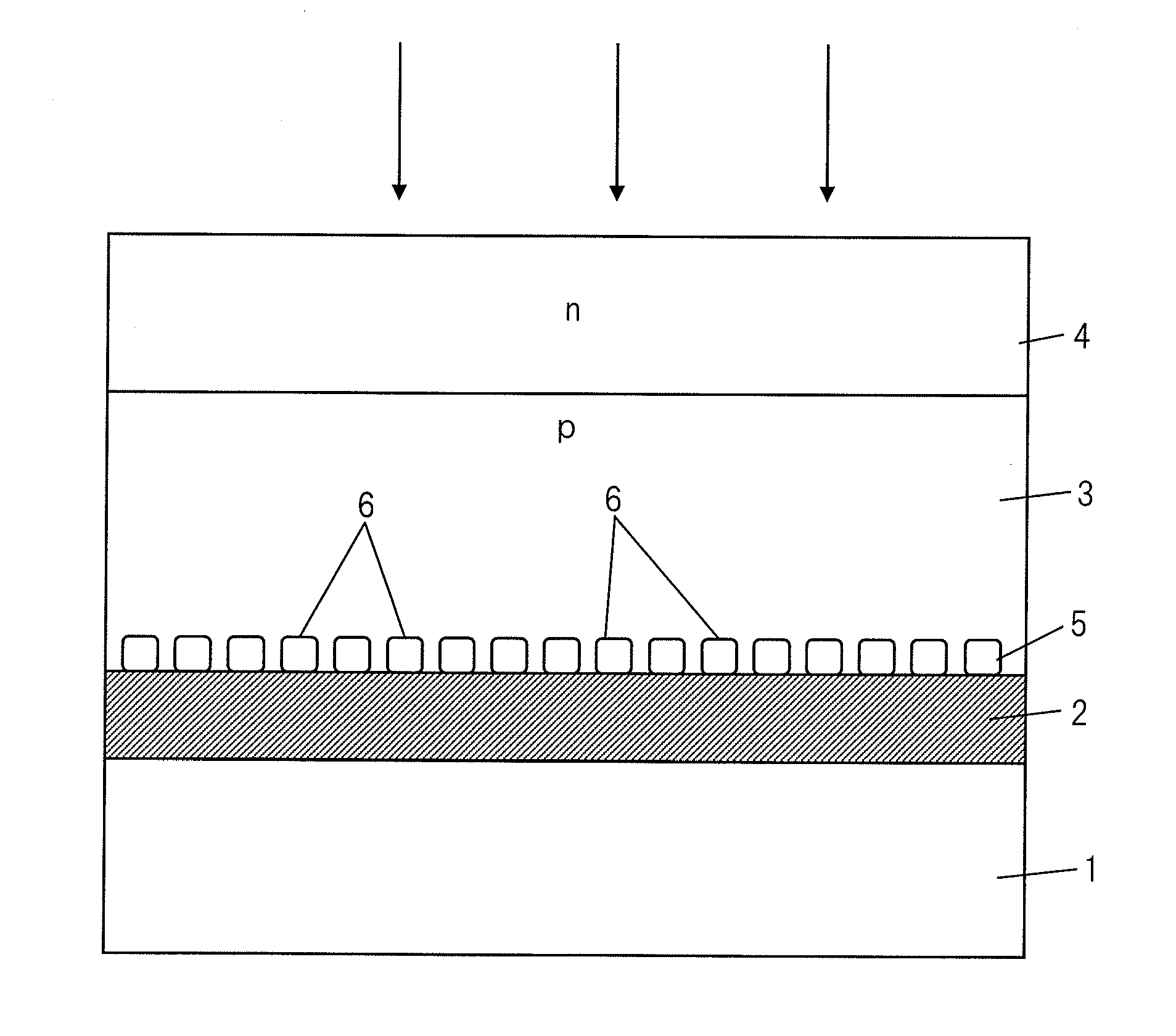
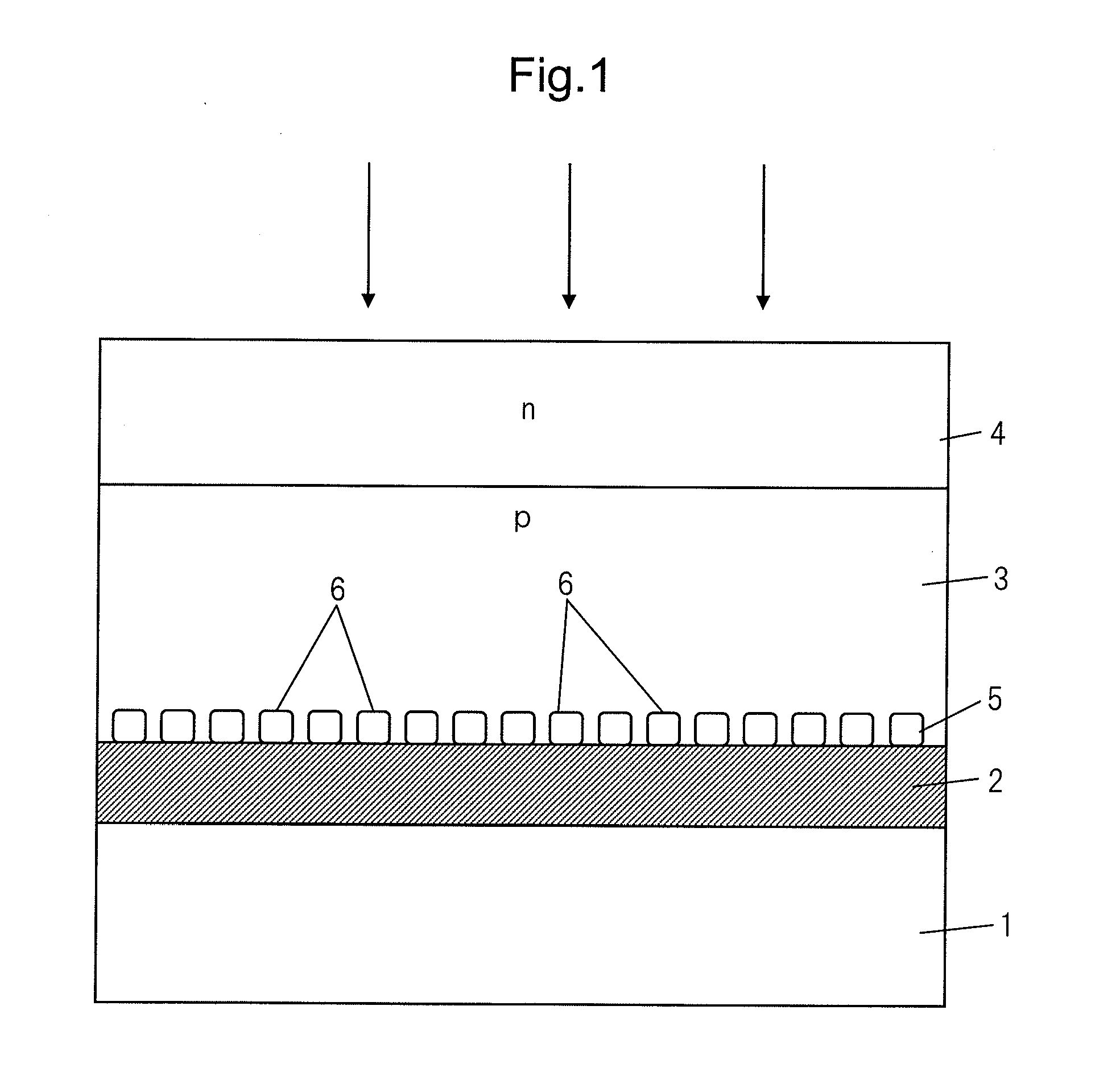
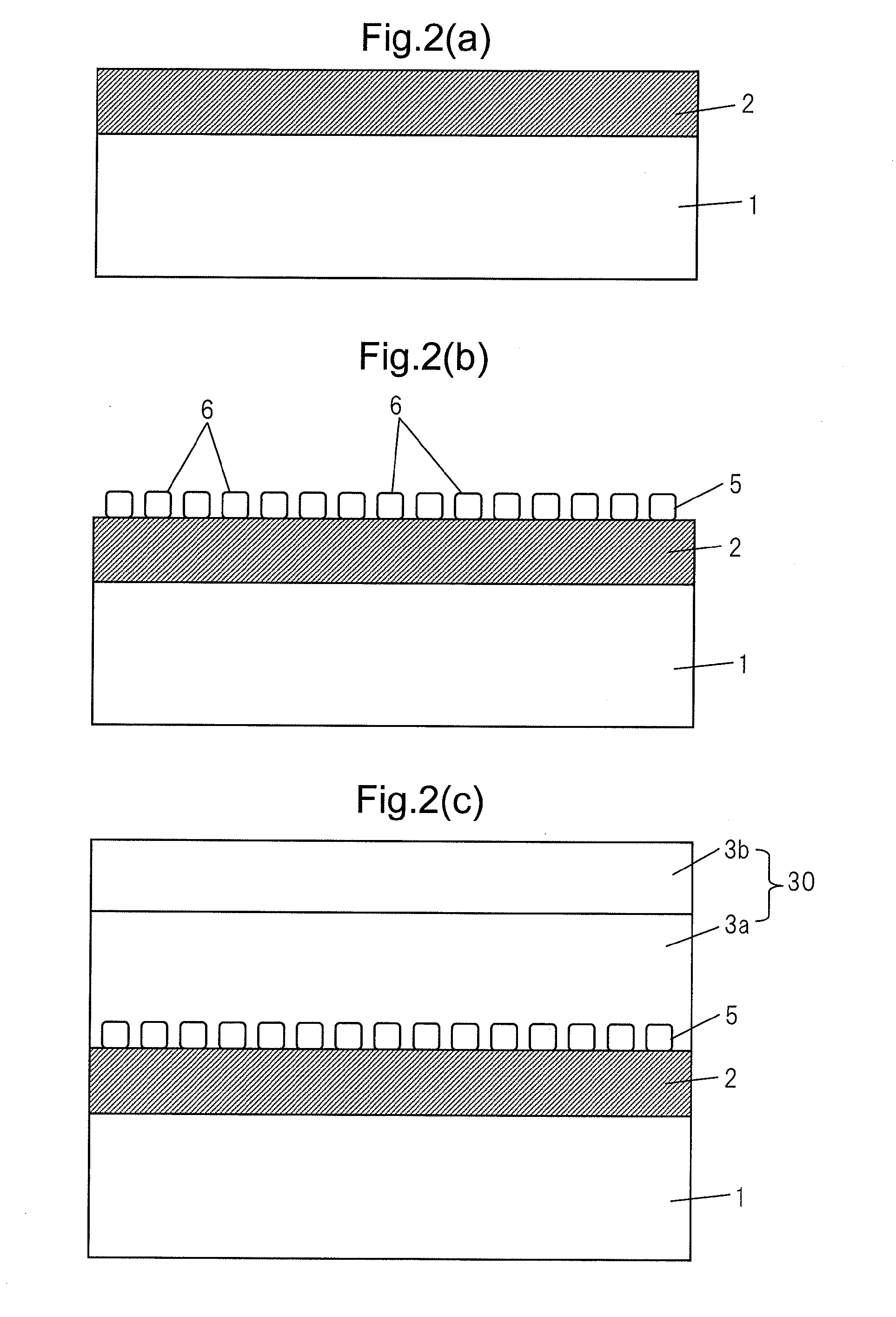
[0031]FIG. 1 is a cross-sectional view which shows the schematic structure of a thin film solar cell of a substrate structure according to the present invention, in particular, the structure of a thin film solar cell which uses a CIS-based semiconductor as the p-type light absorption layer. In the figure, 1 indicates a substrate which is comprised of glass, a plastic, a metal sheet, etc., 2 a metal back surface electrode layer which has Mo, Ti, Cr, etc. as a material, 3 a p-type light absorption layer which is comprised of a CIS-based semiconductor, and 4 an n-type transparent electrode film which has ZnO, ITO, etc. as a material. These form the window layer of this solar cell. Note that, between the p-type light absorption layer 3 and the n-type transparent electrode film 4, a high resistance buffer layer which has Zn(O, S, OH), CdS, In2S3, etc. as its material may be provided. The p-type light absorption layer 3 is comprised of Cu(In, Ga)Se2, Cu(In, Ga)(Se, S)2, CuInS2, etc.

[0032]...

embodiment 2

[0052]FIG. 4 is a cross-sectional view which shows the schematic structure of a super straight structure of a thin film solar cell according to the present invention and, in particular, shows the structure of a thin film solar cell which is comprised of amorphous silicon. In FIG. 4, 10 indicates a glass or other transparent substrate, 11 an ITO or other transparent electrode film, 12 a p-type amorphous silicon layer, 13 an i-type amorphous silicon layer, and 14 an n-type amorphous silicon layer. The transparent electrode film 11 is formed on the substrate by forming an ITO film by sputtering etc. The p-type amorphous silicon layer 12, i-type amorphous silicon layer 13, and n-type amorphous silicon layer 14 configure a light absorption layer and are formed by forming p-, i-, and n-types of amorphous silicon by plasma CVD etc. on the transparent electrode film 11.

[0053]Reference notation 15 shows a nanoparticle dispersed layer which is formed on the n-type amorphous silicon layer 14. ...


PUM

PropertyMeasurementUnit
particle sizeaaaaaaaaaa
thicknessaaaaaaaaaa

Abstract

In the present invention, in order to achieve a point contact, a thin film solar cell has a thin film light absorbing layer (3) disposed between a transparent conducive film (4) and a back-side metal electrode layer (2), and at the interface between the back-side metal electrode layer (2) and the light absorbing layer (3), the thin film solar cell is provided with a nanoparticle dispersion layer (5) including nanoparticles (6, 6 . . . ), where at least the surface of the nanoparticles is an insulator.

Description

REFERENCE TO RELATED APPLICATIONS[0001]This application is the national stage application under 35 USC 371 of International Application No. PCT / JP2012 / 071309, filed Aug. 23, 2012, which claims the priority of Japanese Patent Application No. 2011-191451, filed Sep. 2, 2011, the entire contents of which are incorporated herein by reference.TECHNICAL FIELD OF THE INVENTION[0002]The present invention relates to a thin film solar cell and a method of production of the same, in particular, relates to a thin film solar cell which can achieve a high photovoltaic conversion efficiency and a method of production of the same.BACKGROUND OF THE INVENTION[0003]In recent years, thin film solar cells which use amorphous silicon or chalcogenide-based compounds as materials have come under the spotlight. Such solar cells have the superior properties of being inexpensive in cost of materials and enabling easy production of large-sized solar cell panels. On the other hand, in general, their photovoltai...

Claims


Application Information

Patent Timeline
Patent Type & Authority Applications(United States)
IPC IPC(8): H01L31/0224H01L31/0216
CPCH01L31/02167H01L31/022441H01L31/022425H01L31/02366H01L31/03923H01L31/03925Y02E10/541H01L31/056Y02E10/52H01L31/0749H01L31/075Y02E10/548Y02P70/50
Inventor SUGIMOTO, HIROKI
Owner SOLAR FRONTIER
Why Eureka
Try Eureka