
Microbially-mediated method for synthesis of non-oxide semiconductor nanoparticles

a non-oxide semiconductor and nanoparticle technology, applied in the direction of transportation and packaging, metal selenides/tellurides, chemistry apparatus and processes, etc., can solve the problems of prohibitively expensive physical techniques are typically not useful for synthesizing semiconductor nanoparticles in commercially significant quantities, and the cost of commercially significant amounts of resulting nanoparticles is prohibitively high. , to achieve the effect of non-prohibi

Active Publication Date: 2014-08-07
UNIV OF TENNESSEE RES FOUND +1
View PDF3 Cites 3 Cited by
  • Summary
  • Abstract
  • Description
  • Claims
  • Application Information

AI Technical Summary

Benefits of technology

[0012]In one aspect, the invention is directed to a microbially-mediated method for the production of semiconductor nanoparticles. The method described herein can advantageously produce a variety of semiconductor nanoparticle compositions on a commercially viable scale. In addition, the method can advantageously produce semiconductor nanoparticles of a particular particle size, morphology, electronic or photonic characteristic, dopant composition, or doping level. In particular embodiments, the semiconductor nanoparticles described herein are useful as photovoltaic materials, as used, for example, in solar cell devices.
[0019]The invention advantageously provides a method capable of producing pure semiconductor nanoparticles on a commercial (i.e., bulk) scale at a non-prohibitive cost. A further particular advantage of the method is that it provides the capability of synthesizing semiconductor nanoparticles having selected photoluminescent characteristics over a wide range of such characteristics. For example, by controlling the size, shape, composition, and / or crystalline structure of the nanoparticles, the location or width of the photoluminescence peak can be accordingly controlled or fine-tuned over a wide range.
[0020]Numerous electronic and photonic devices can benefit from such precise control of the photoluminescent properties of semiconductor nanoparticles. In particular, photovoltaic devices are currently limited by the use of photoluminescent materials that are not tunable, or semi-tunable with great difficulty. Yet, there is a clear and present need in the art of photovoltaic devices for photoluminescent-tunable materials. Other types of devices that can benefit from such tunable materials include light-emitting and laser diodes. Accordingly, the method and compositions of the invention can greatly advance several types of devices, including photovoltaic devices.

Problems solved by technology

The physical techniques are typically not useful for synthesizing semiconductor nanoparticles in commercially significant quantities (e.g., grams or kilograms).
Though the chemical processes described above are generally capable of producing semiconductor nanoparticles in more significant quantities, the processes are generally energy intensive (e.g., by generally requiring heating and a post-annealing step), and hence, costly.
Accordingly, commercially significant amounts of the resulting nanoparticles tend to be prohibitively expensive.
Furthermore, these processes tend to be significantly limited with respect to control of the physical (e.g., size, shape, and crystalline form) and electronic or photonic characteristics of the resulting nanoparticles.
However, there are significant obstacles that prevent such microbially-mediated methods from being commercially viable.
For example, current microbial methods are generally limited to the production of semiconductor nanoparticles on a research scale, i.e., an amount sufficient for elucidation by analytical methods.

Method used


Image

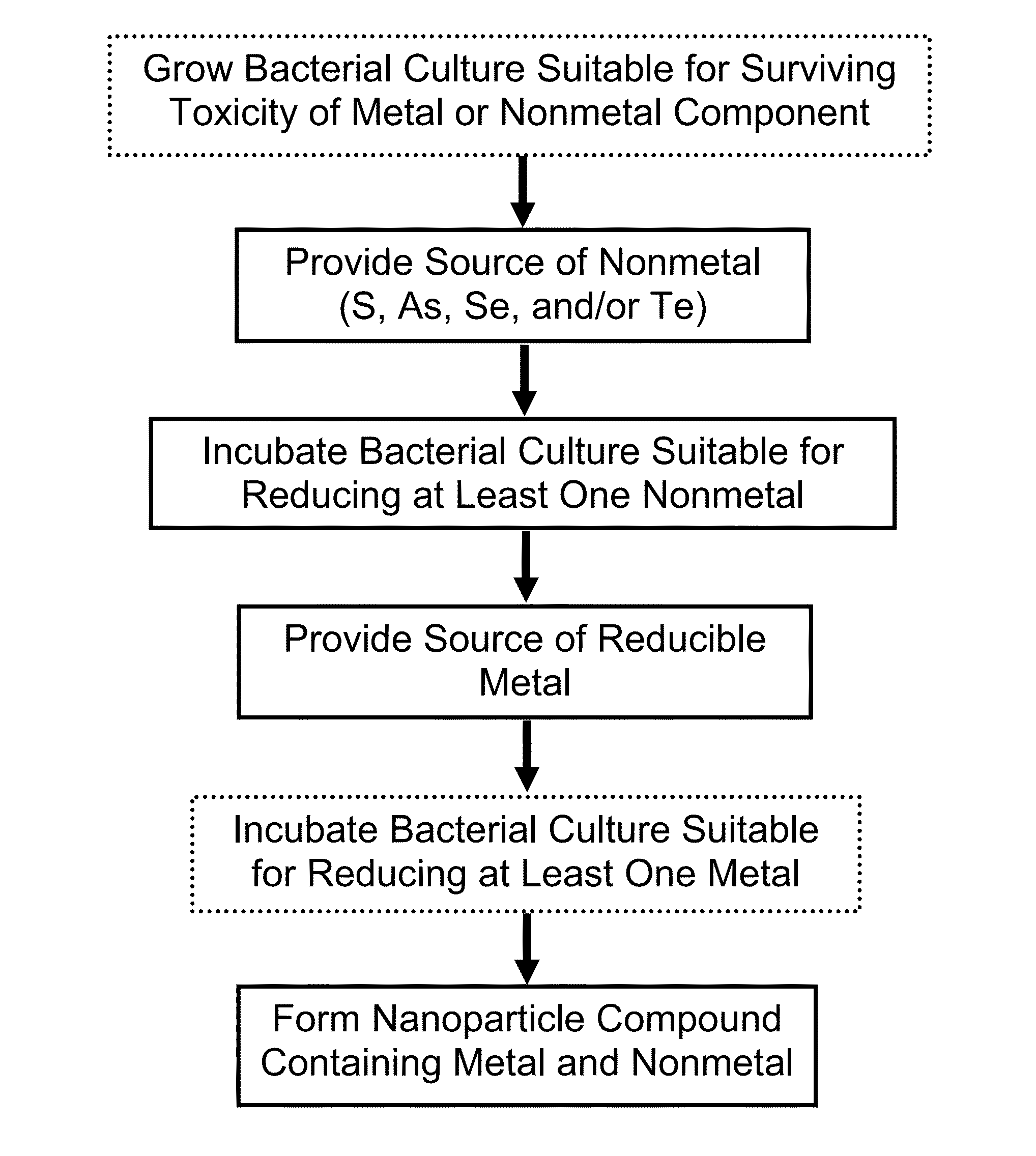
  • Microbially-mediated method for synthesis of non-oxide semiconductor nanoparticles
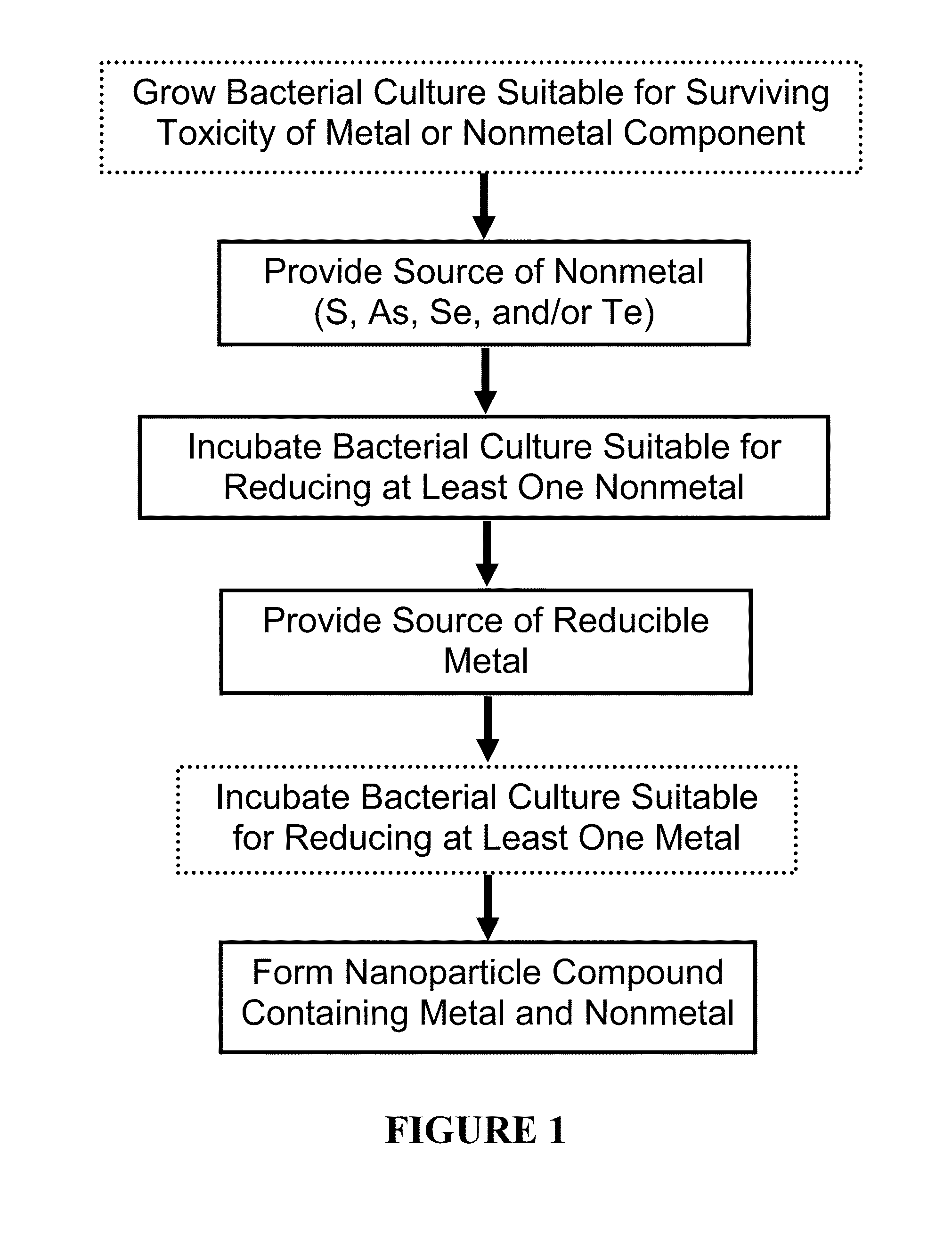
  • Microbially-mediated method for synthesis of non-oxide semiconductor nanoparticles
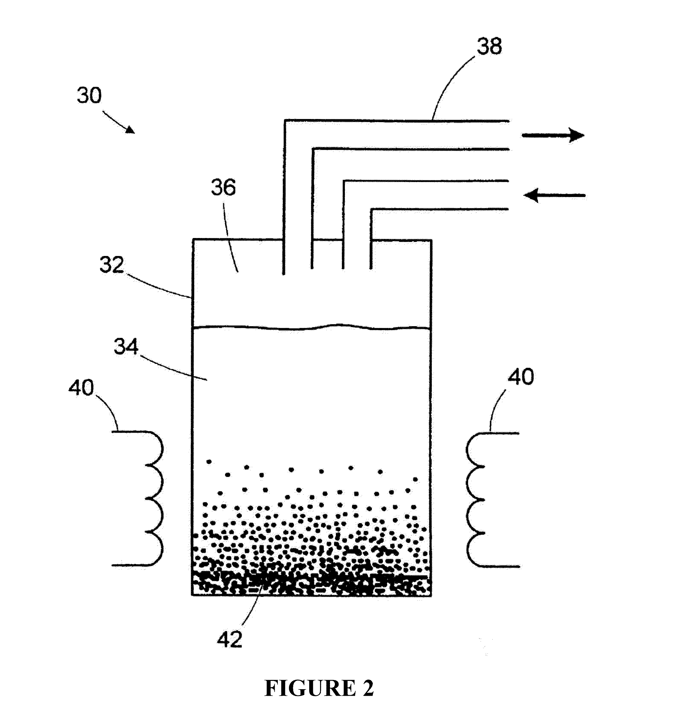
  • Microbially-mediated method for synthesis of non-oxide semiconductor nanoparticles

Examples


example 1

Preparation of ZnS Nanoparticles Using Sulfate-Reducing Microbes

[0115]A mesophilic sulfate-reducing strain Desulfovibrio G-20 was grown in a lactate / SO4 culture medium as taught generally by Li et al., “Reduction of iron oxides enhanced by a sulfate-reducing bacterium and biogenic H2S”, Geomicrobiol. J., 23:103-117 (2006), the entire disclosure of which is incorporated herein by reference. Zn2+ was added as ZnCl2 at 0.2 mM and well-formed highly crystalline ZnS (sphalerite phase) nanoparticles were formed. Precipitated semi-conductor materials were harvested by repeated centrifugation followed by one or more times of washing with deionized water. Particle size was estimated at approximately 5.9 nm A similar experimental run using standard medium containing nutrients, vitamins, trace elements, lactate as an electron donor at 50 mM, and Na2SO4 as a non-metal component with 50 mM and with Zn2+ added as ZnCl2 at 5 mM yielded ZnS particles estimated at approximately 3.7 nm in size.

[0116]...

example 2

Preparation of CdS Nanoparticles Using Sulfate-Reducing Microbes

[0117]CdS nanoparticles were synthesized using the same mesophilic sulfate-reducing strain Desulfovibrio G-20. In this case, CdCl2 as a precursor metal component was added at 0.06 mM and a sulfur-containing non-metal compound as 0.06 mM Na2SO3 based on CO3-buffered medium containing nutrients, vitamins, trace elements, and lactate as an electron donor at 50 mM. Precipitated nanoparticles were harvested by repeated centrifugation followed by one or more times washing with deionized water. Well-formed highly crystalline CdS nanoparticles with an extremely sharp photoluminescent peak characterized by a full-width half maximum value of or less than 20 nm, as shown in FIG. 5C, were formed.

[0118]The foregoing example demonstrates that the sulfate-reducing strain G-20 was able to make the target CdS phase in the desired size range. Remarkably, the process showed no deleterious toxicity of Cd on the bacteria used. Again, the pr...

example 3

Preparation of ZnS Nanoparticles Using Metal-Reducing Microbes

[0119]In an effort to demonstrate the generality of the process, the following series of experiments were performed using a metal-reducing strain of bacteria rather than a sulfate-reducing strain. Fluorescent ZnS nanoparticles were synthesized using the thermophilic metal-reducing strain TOR-39 cultured in low-NaCl medium for one month. Because TOR-39 cannot efficiently reduce sulfate per se, sulfur-containing non-metal component was added in the form of thiosulfate. Zn was added as ZnCl2. One experiment used 5 mM thiosulfate and 5 mM ZnCl2, added as sequential aliquots (1 mM / day). A second experiment used 10 mM thiosulfate and 10 mM ZnCl2, added as sequential aliquots (1 mM / day). The two experiments produced highly crystalline ZnS quantum dots with average particle sizes of 6.5 nm and 12 nm, respectively.

[0120]This surprising result may be interpreted as follows. Although TOR-39 is a metal-reducing bacterium (e.g., typic...


PUM

PropertyMeasurementUnit
compositionaaaaaaaaaa
photoluminescent peakaaaaaaaaaa
semiconductoraaaaaaaaaa

Abstract

The invention is directed to a method for producing non-oxide semiconductor nanoparticles, the method comprising: (a) subjecting a combination of reaction components to conditions conducive to microbially-mediated formation of non-oxide semiconductor nanoparticles, wherein said combination of reaction components comprises i) anaerobic microbes, ii) a culture medium suitable for sustaining said anaerobic microbes, iii) a metal component comprising at least one type of metal ion, iv) a non-metal component comprising at least one non-metal selected from the group consisting of S, Se, Te, and As, and v) one or more electron donors that provide donatable electrons to said anaerobic microbes during consumption of the electron donor by said anaerobic microbes; and (b) isolating said non-oxide semiconductor nanoparticles, which contain at least one of said metal ions and at least one of said non-metals. The invention is also directed to non-oxide semiconductor nanoparticle compositions produced as above and having distinctive properties.

Description

CROSS REFERENCE TO RELATED APPLICATIONS[0001]This application is a divisional of copending application Ser. No. 12 / 874,522 filed Sep. 2, 2010 which is a continuation-in-part of copending application Ser. No. 12 / 364,638 filed Feb. 3, 2009, all of the contents of which are incorporated herein by reference.[0002]This invention was made with government support under Contract Number DE-AC05-00OR22725 between the United States Department of Energy and UT-Battelle, LLC. The United States government has certain rights in this invention.FIELD OF THE INVENTION[0003]The present invention relates to the field of microbial synthesis of inorganic materials, and more particularly, microbial synthesis of non-oxide semiconductor nanoparticles.BACKGROUND OF THE INVENTION[0004]Nanoparticles having metal non-oxide compositions (i.e., “semiconductor” or “quantum dot” nanoparticles) are increasingly being used in numerous emerging applications. Some of these applications include electronics (e.g., transi...

Claims


Application Information

Patent Timeline
Patent Type & Authority Applications(United States)
IPC IPC(8): C12P3/00H01L31/0352H01L31/032
CPCC12P3/00H01L31/035218H01L31/0326C01B17/20C01B19/007C01G9/08C01G11/02C01G15/006C01G19/006C01P2002/72C01P2002/82C01P2002/84C01P2004/04C01P2006/40Y10T428/2982
Inventor PHELPS, TOMMY J.LAUF, ROBERT J.MOON, JI-WONRONDINONE, ADAM JUSTINLOVE, LONNIE J.DUTY, CHAD EDWARDMADDEN, ANDREW STEPHENLI, YILIANGIVANOV, ILIA N.RAWN, CLAUDIA JEANETTE
Owner UNIV OF TENNESSEE RES FOUND
Learn More