Semiconductor device and method of manufacturing the same

a technology of thin-film resistor and semiconductor device, which is applied in the direction of semiconductor device details, semiconductor/solid-state device details, capacitors, etc., can solve the problems of increasing cost, affecting the efficiency of manufacturing process, and damage to the top of the thin-film resistor, so as to achieve the effect of reducing damage, increasing cost, and inevitably worsening efficiency of manufacturing process

Active Publication Date: 2014-08-28
ROHM CO LTD
View PDF3 Cites 14 Cited by
  • Summary
  • Abstract
  • Description
  • Claims
  • Application Information

AI Technical Summary

Benefits of technology

[0012]If a contact is formed on the thin-film resistor from above, as in Patent Documents 1 and 2, it is necessary to form a via hole (contact hole) that reaches the thin-film resistor by selectively etching the interlayer insulating film. Therefore, there is a risk that the top of the thin-film resistor could be damaged by being exposed to etching gas, the etchant, or the like. If wet etching is used, as in Patent Document 2, the damage may be slightly reduced, but a separate etching mask is then necessary to form the via hole to the thin-film resistor. As a result, the efficiency of the manufacturing process is inevitably worsened and the cost is increased.

Problems solved by technology

Therefore, there is a risk that the top of the thin-film resistor could be damaged by being exposed to etching gas, the etchant, or the like.
As a result, the efficiency of the manufacturing process is inevitably worsened and the cost is increased.
However, the barrier film of the wiring line contacting the via below is a material that has the same resistance as the thin-film resistor; thus, there is a risk that variation in contact resistance will occur between the via and the wiring line.
Furthermore, if it is necessary to remove a primary part of the wiring line (Al alloy wiring, for example) from the area above the thin-film resistor used for resistance, then there is a risk the thin-film resistor could be damaged during etching to remove this.
If the thin-film resistor is formed on the wiring line pattern, as in Patent Document 3, differences in thickness of the wiring line can appear on the thin-film resistor, and therefore, there is a risk that deviation will occur in the resistance of the thin-film resistor.

Method used


Image

  • Semiconductor device and method of manufacturing the same
  • Semiconductor device and method of manufacturing the same
  • Semiconductor device and method of manufacturing the same

Examples


embodiment 1

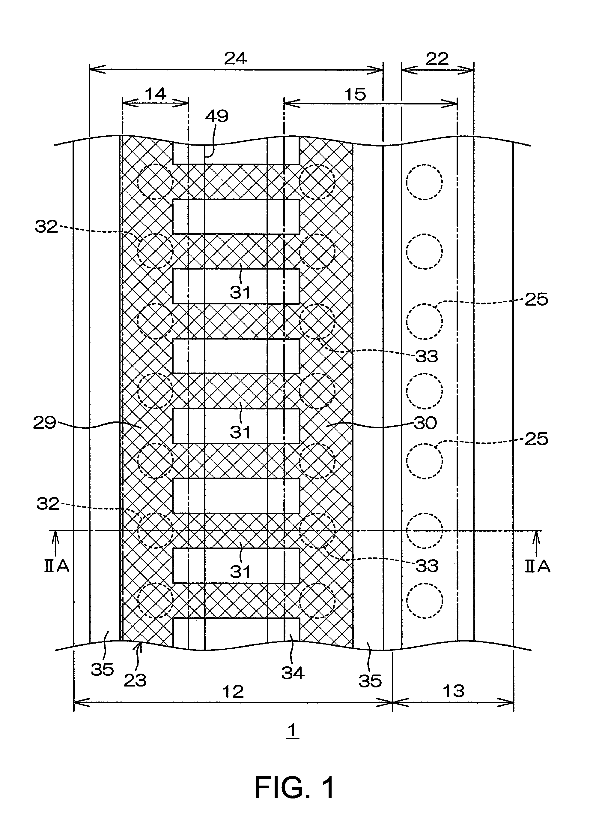
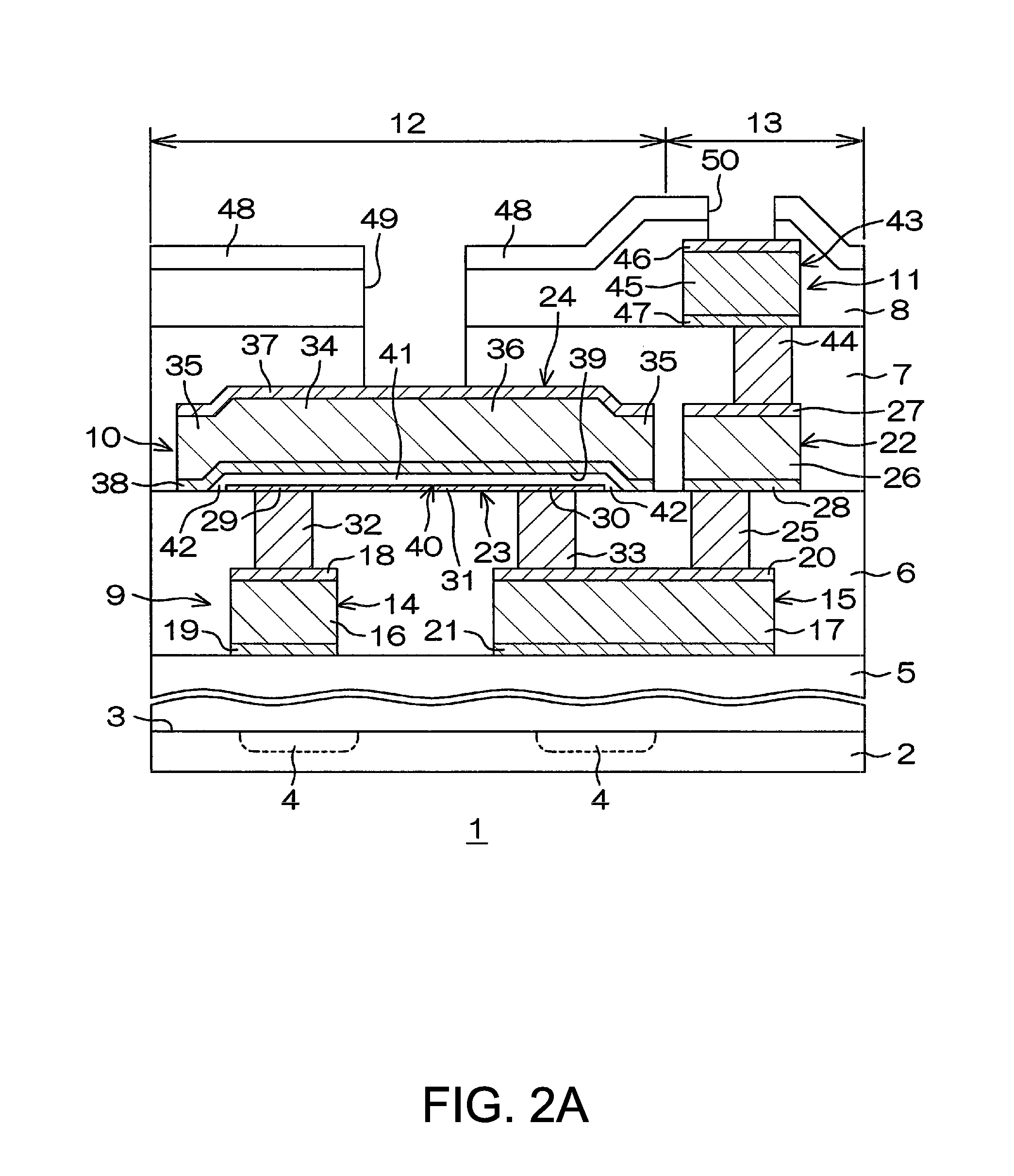
[0093]FIG. 1 is a plan view of a semiconductor device 1 of the present invention. FIG. 2A is a cross-sectional view ofFIG. 1 cut along IIA-IIA. FIG. 2B is a view of the semiconductor device 1 after laser trimming.

[0094]The semiconductor device 1 includes a semiconductor substrate 2, and a plurality of interlayer insulating films 5 to 8 layered on this semiconductor substrate 2. The semiconductor substrate 2 is a silicon substrate in which semiconductor elements 4 such as active and passive elements are embedded in a surface 3 thereof, for example.

[0095]In the present embodiment, the plurality of interlayer insulating films 5 to 8 include, in order from the surface 3 of the semiconductor substrate 2: the first interlayer insulating film 5, the second interlayer insulating film 6 that is one example of a second interlayer insulating film of the present invention, the third interlayer insulating film 7 that is one example of an interlayer insulating film of the present invention, and ...

embodiment 2

[0138]FIG. 4 is a cross-sectional view of a semiconductor device 59 of the present invention. In FIG. 4, portions corresponding to the portions in FIG. 2A are assigned the same reference characters.

[0139]This semiconductor device 59 further includes a TiN layer 60 between a dummy wiring line 24 and an insulating film 40, in addition to the configuration of the semiconductor device 1 described above. In a plan view, the TiN layer 60 is formed in a thin-film shape having the same outer shape as a thin-film resistor 23. In other words, in FIG. 1, the TiN layer 60 has a shape in which the areas between adjacent fuses 31 of the ladder-like thin-film resistor 23 are also formed in a film-like shape. This TiN layer 60 faces the thin-film resistor 23 across the plane part 41 of the insulating film 40.

[0140]The manufacturing steps of the semiconductor device 59 of this embodiment are substantially similar to the steps shown in FIGS. 3A to 3K. However, in the step in FIG. 3B, a TiN material ...

embodiment 3

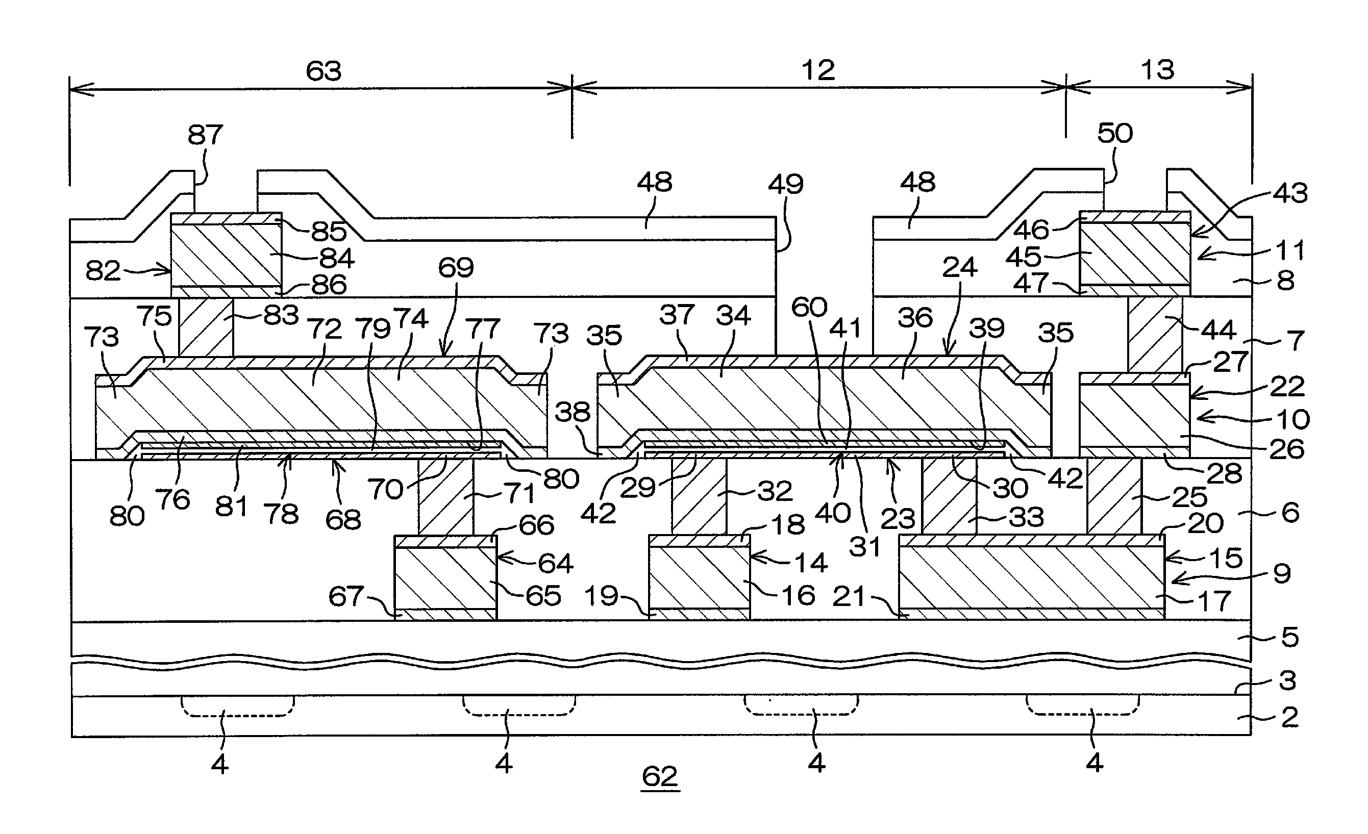
[0146]FIG. 6 is a plan view of a semiconductor device 62 of the present invention. FIG. 7 is a cross-sectional view of FIG. 6 cut along VII-VII. In FIGS. 6 and 7, portions corresponding to the portions in FIGS. 1, 2A, and 4 are assigned the same reference characters.

[0147]This semiconductor device 62 further includes a capacitor area 63 on an area on a semiconductor substrate 2, in addition to the above-mentioned configuration of the semiconductor devices 1 and 59. The capacitor area 63 is selectively configured so as to be adjacent to a side of a resistor area 12 that is opposite to a wiring area 13.

[0148]In the capacitor area 63, a second wiring layer 9 includes a wiring line 64. The wiring line 64 is formed with approximately the same width as a wiring line 14 in the resistor area 12, and this wiring line 64 is parallel to the wiring line 14 along the boundary of the resistor area 12 and capacitor area 63. The wiring line 64 is electrically connected to semiconductor elements 4 ...


PUM


Abstract

A semiconductor device has a resistor area and wiring area selectively disposed on a semiconductor substrate. In this semiconductor device, a second interlayer insulating film is formed above the semiconductor substrate, and a thin-film resistor is disposed on the second interlayer insulating film in the resistor area. Vias that contact the thin-film resistor from below are formed in the second interlayer insulating film. A wiring line is disposed on the second interlayer insulating film in the wiring area. A dummy wiring line that covers the thin-film resistor from above is disposed in a third wiring layer that is in the same layer as the wiring line, and an insulating film is interposed between the thin-film resistor and the dummy wiring line.

Description

[0001]This application claims the benefit of Japanese Application No. 2013-37578, filed in Japan on Feb. 27, 2013, which is hereby incorporated by reference in its entirety.BACKGROUND OF THE INVENTION[0002]1. Field of the Invention[0003]The present invention relates to a semiconductor device having a thin-film resistor and a method of manufacturing this semiconductor device.[0004]2. Description of Related Art[0005]In high-performance analog devices, it is necessary to have passive parts including thin-film resistors (TaN, SiCr, or the like, for example) that are capable of being laser trimmed. Examples of semiconductor devices provided with thin-film resistors are respectively disclosed in Patent Documents 1 to 3, for example.[0006]Disclosed in Patent Document 1 is a semiconductor device that includes a thin-film resistor formed on a semiconductor substrate, a middle metal layer formed so as to cover the thin-film resistor, an insulating film formed so as to cover the middle metal l...

Claims


Application Information

Patent Timeline
Patent Type & Authority Applications(United States)
IPC IPC(8): H01L23/522H01L49/02
CPCH01L23/5228H01L23/5223H01L28/20H01L28/40H01L23/522H01L23/5258H01L23/53223H01L27/016H01L28/24H01L28/60H01L2924/0002H01L2924/00H01L21/76805H01L21/76829H01L21/7687H01L23/5226H01L23/528H01L23/5329
Inventor NISHIMURA, LSAMUMIFUJI, MICHIHIKONISHIO, KAZUMASA
Owner ROHM CO LTD
Why Eureka
Try Eureka