Optical-to-electrical converter unit and semiconductor light-receiving device

a technology of optical-to-electrical converter and semiconductor light-receiving device, which is applied in the direction of optics, optical elements, instruments, etc., can solve the problem that the semiconductor light-receiving device is difficult to operate stably, and achieve the effect of reducing the parametric capacitance generated between the back electrode and the semiconductor layer

Active Publication Date: 2014-09-04
SUMITOMO ELECTRIC IND LTD
View PDF2 Cites 10 Cited by
  • Summary
  • Abstract
  • Description
  • Claims
  • Application Information

AI Technical Summary

Benefits of technology

[0013]For example, when a back electrode is formed on the entire back surface of the substrate and the light-receiving element and the optical waveguide include semiconductor layers of the same conductivity type formed on the front surface of the substrate, a parasitic capacitance is generated between the back electrode and the semiconductor layers. In this case, a transmission path of an electrical signal generated in the light-receiving element through the parasitic capacitance is formed, and a problem of cross talk arises between the light-receiving elements. In the optical-to-electrical converter unit described above, the back electrode includes a first back electrode portion formed in the first region and a second back electrode portion formed in the second region. In the first region of the substrate, the via electrode is formed, and in the second region of the substrate, the light-receiving element and the optical waveguide unit are formed. The first back electrode portion is electrically connected to the via electrode, and the first back electrode portion and the second back electrode portion are electrically isolated from each other. Accordingly, a parasitic capacitance generated between the back electrode and the semiconductor layers is reduced. Even when the light-receiving element and the optical waveguide unit include semiconductor layers of the same conductivity type formed on the front surface of the substrate, a transmission path of an electrical signal generated in the light-receiving element through the parasitic capacitance is not formed. Thus, the problem of cross talk among the light-receiving elements can be alleviated.

Problems solved by technology

For example, if there is a resonance frequency of the circuit in the band of the operation frequency of the semiconductor light-receiving device, it becomes difficult for the semiconductor light-receiving device to operate stably.

Method used


Image

  • Optical-to-electrical converter unit and semiconductor light-receiving device
  • Optical-to-electrical converter unit and semiconductor light-receiving device
  • Optical-to-electrical converter unit and semiconductor light-receiving device

Examples


example 1

, and

[0039]FIG. 21 is a circuit diagram showing electrical connections in a semiconductor light-receiving device according to Comparative Example.

DESCRIPTION OF THE PREFERRED EMBODIMENTS

[0040]Embodiments for carrying out the present invention will now be described in detail with reference to the attached drawings. In the description of the drawings, the same elements are represented by the same reference characters and the descriptions therefor are omitted to avoid redundancy.

first embodiment

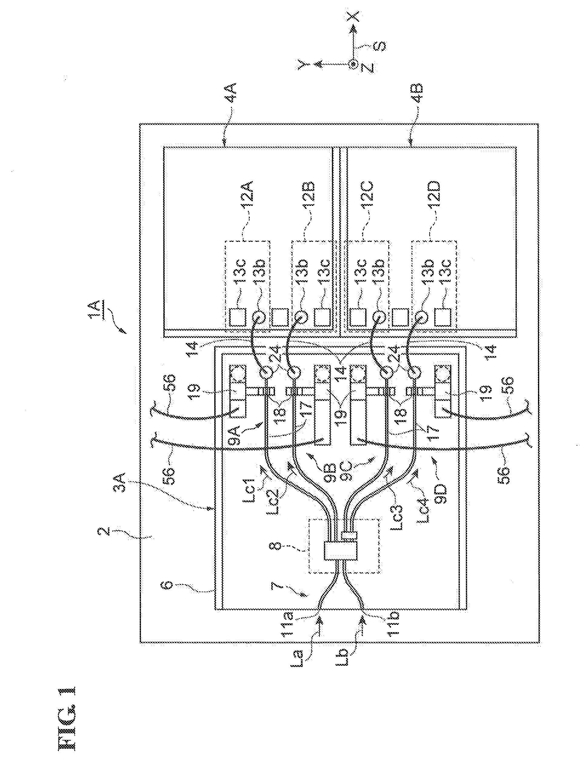
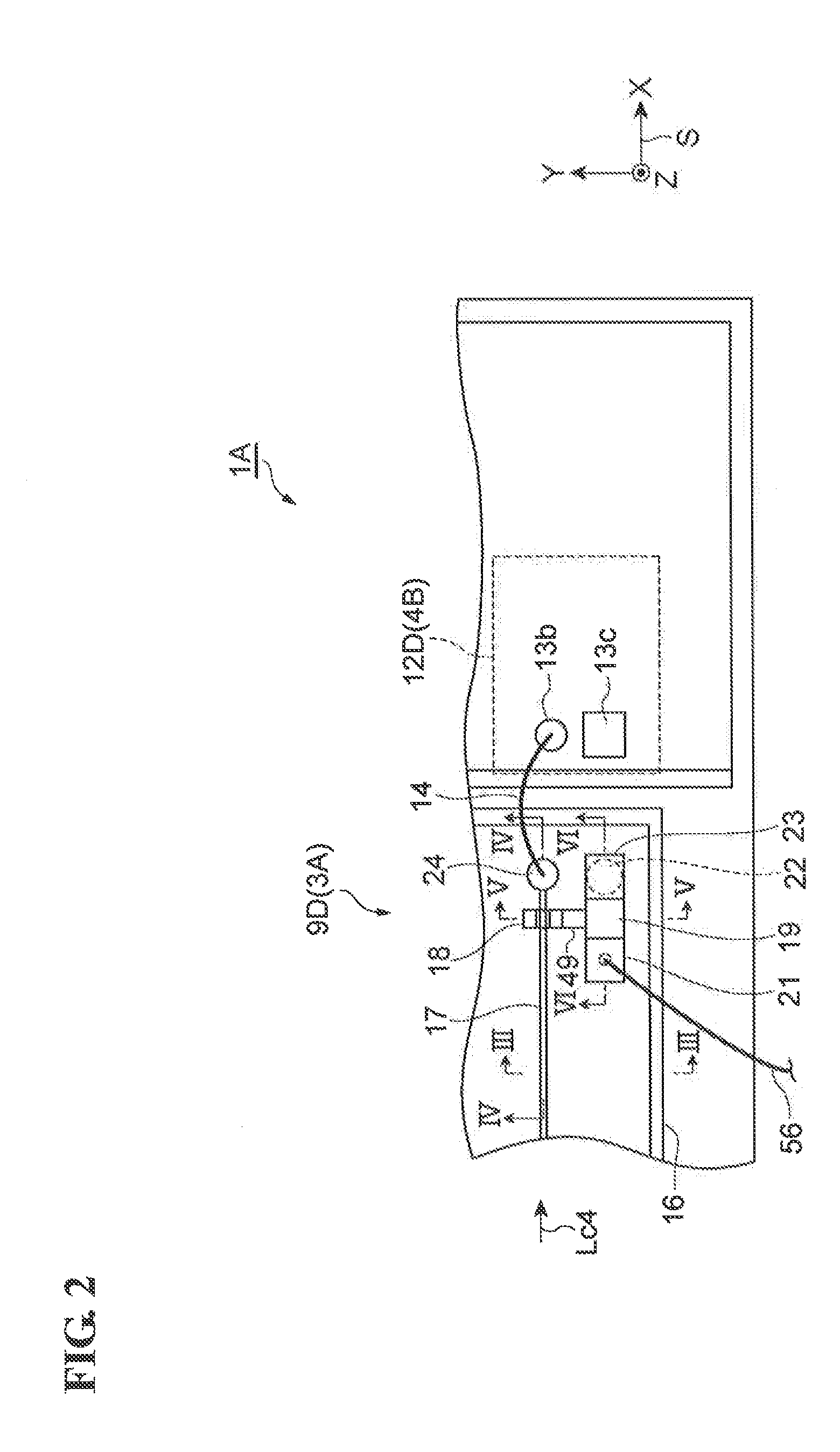
[0041]An optical waveguide-type semiconductor light-receiving device (hereinafter may be simply referred to as “light-receiving device”) according to a first embodiment is described with reference to FIGS. 1 to 7. FIG. 1 is a plan view of an optical waveguide-type semiconductor light-receiving device according to a first embodiment. FIG. 2 is a partial enlarged view of the semiconductor light-receiving device according to the first embodiment. FIG. 3 is a cross-sectional view taken along line III-III in FIG. 2. FIG. 4 is a cross-sectional view taken along line IV-IV in FIG. 2. FIG. 5 is a cross-sectional view taken along line V-V in FIG. 2. FIG. 6 is a cross-sectional view taken along line VI-VI in FIG. 2. FIG. 7 is a circuit diagram showing electrical connections in the semiconductor light-receiving device according to the first embodiment. For the sake of convenience, an orthogonal coordinate system S is included in each drawing.

[0042]In recent years, optical communication systems...

second embodiment

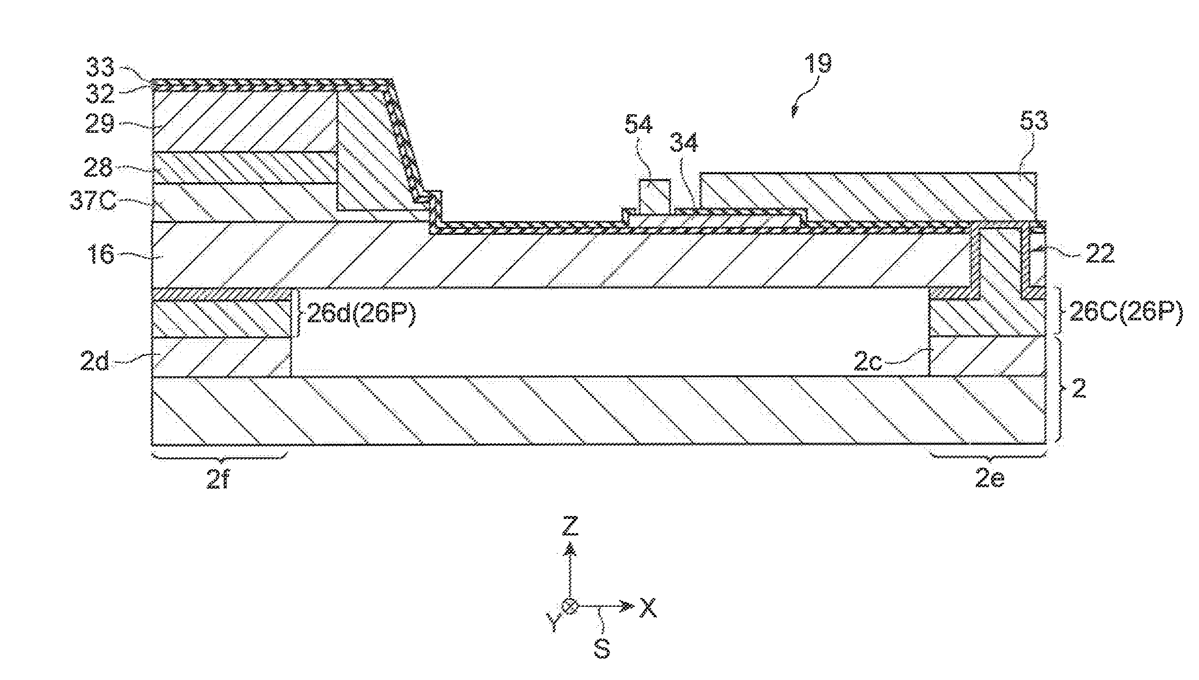
[0086]An optical waveguide-type semiconductor light-receiving device 1B according to a second embodiment will now be described with reference to FIGS. 13 and 14. FIG. 13 is a cross-sectional view of the semiconductor light-receiving device 1B. The cross section (XZ plane) of the O / E converter 9D taken in the waveguiding direction (X direction) is shown in FIG. 13. FIG. 14 is a cross-sectional view of the semiconductor light-receiving device 1B. The cross section (YZ plane) of the O / E converter 9D perpendicular to the waveguiding direction (X direction) is shown in FIG. 14. The semiconductor light-receiving device 1B differs from the light-receiving device 1A in that it has a back electrode 26B having a structure different from that of the back electrode 26 of the light-receiving device 1A. In particular, the back electrode 26 of the light-receiving device 1A is formed over the entire back surface 16b of the substrate 16. In contrast, the back electrode 26B of the semiconductor light...


PUM


Abstract

An optical-to-electrical converter unit includes a substrate having front and back surfaces; an optical waveguide unit; and an optical-to-electrical converter. The optical-to-electrical converter includes a light-receiving element optically coupled to the optical waveguide unit; a capacitance element including first and second conductive layers and an insulating layer disposed between the first and second conducive layers; an electrode pad electrically connected to the light-receiving element; a back electrode formed on the back surface of the substrate; and a via electrode extending from the front surface to the back surface of the substrate. The optical waveguide unit, the light-receiving element, the capacitance element, and the electrode pad are formed on the front surface. The first conductive layer of the capacitance element is electrically connected to the light-receiving element and the electrode pad. The second conductive layer of the capacitance element is electrically connected to the back electrode through the via electrode.

Description

BACKGROUND OF THE INVENTION[0001]1. Field of the Invention[0002]The present invention relates to an optical-to-electrical converter unit and a semiconductor light-receiving device.[0003]2. Description of the Related Art[0004]In recent years, waveguide-type semiconductor light-receiving devices in which photodiodes and optical waveguides are integrated on semiconductor substrates have been studied. Such semiconductor light-receiving devices have high frequency characteristics which make them capable of responding to optical signals having high bit rates such as 40 Gb / s or higher, for example. Because of the high frequency characteristics, they are used as receiver front ends of optical transmission systems combining multi-level light intensity modulation systems and digital coherent receiving systems. The semiconductor light-receiving device is fabricated by forming, on a semiconductor substrate, a butt-joint structure including a stacked semiconductor layer section that constitutes ...

Claims


Application Information

Patent Timeline
Patent Type & Authority Applications(United States)
IPC IPC(8): H01L31/0232
CPCH01L31/02327G02B6/4202H01L31/105
Inventor YONEDA, YOSHIHIROMASUYAMA, RYUJIYAGI, HIDEKIINOUE, NAOKO
Owner SUMITOMO ELECTRIC IND LTD
Why Eureka
Try Eureka