Semiconductor device and fabrication method thereof

a technology of semiconductor devices and fabrication methods, applied in the direction of semiconductor devices, basic electric elements, electrical appliances, etc., can solve the problems of short channel effect, high risk of subthreshold leakage, and device performance degradation of semiconductor devices

Active Publication Date: 2022-10-25
SEMICON MFG INT (SHANGHAI) CORP +1
View PDF3 Cites 0 Cited by
  • Summary
  • Abstract
  • Description
  • Claims
  • Application Information

AI Technical Summary

Benefits of technology

[0026]The disclosed embodiments of the present disclosure may have following beneficial effects. When forming the fin, the gate structure across the fin, and the source-drain doped layer in the fin on both sides of the gate structure over the substrate, the dielectric layer covering the top of the gate structure may be formed over the substrate. A first through-hole may be formed in the dielectric layer on the side (e.g., a side of source region) of the gate structure between the fins in the fin sparse region. The bottom of the first through-hole may expose the top sidewall of the gate structure, and the depth of the first through-hole may be substantially small. When subsequently filling the first through-hole with the metal layer, the volume of the metal layer filled in the first through-hole may be reduced. Therefore, the parasitic capacitance generated between the gate structure and the junction of the source-drain doped layers may be reduced, thereby improving the device performance and quality of the formed semiconductor device, and improving the sensitivity.

Problems solved by technology

However, as a channel length of a device keeps shrinking, the channel control capability of a gate structure deteriorates, and there is increasing difficulty in pinching the channel off by a gate voltage, resulting in a higher risk of subthreshold leakage, that is, the so-called short-channel effect (SCE).
Consequently, the device performance of the semiconductor device may be degraded.
However, as the size of the semiconductor device shrinks and device density increases, the process difficulty of forming the FinFET increases, and the device performance of the formed FinFET is unstable.

Method used


Image

  • Semiconductor device and fabrication method thereof
  • Semiconductor device and fabrication method thereof
  • Semiconductor device and fabrication method thereof

Examples


Embodiment Construction

[0031]Reference will now be made in detail to exemplary embodiments of the disclosure, which are illustrated in the accompanying drawings. Wherever possible, the same reference numbers will be used throughout the drawings to refer to the same or the alike parts.

[0032]For an existing semiconductor device, the parasitic capacitance generated between the gate structure and the junction of the source-drain doped layers is substantially large, which seriously affects the device performance of the semiconductor device. FIGS. 1-11 illustrate semiconductor structures corresponding to certain stages for forming the semiconductor device.

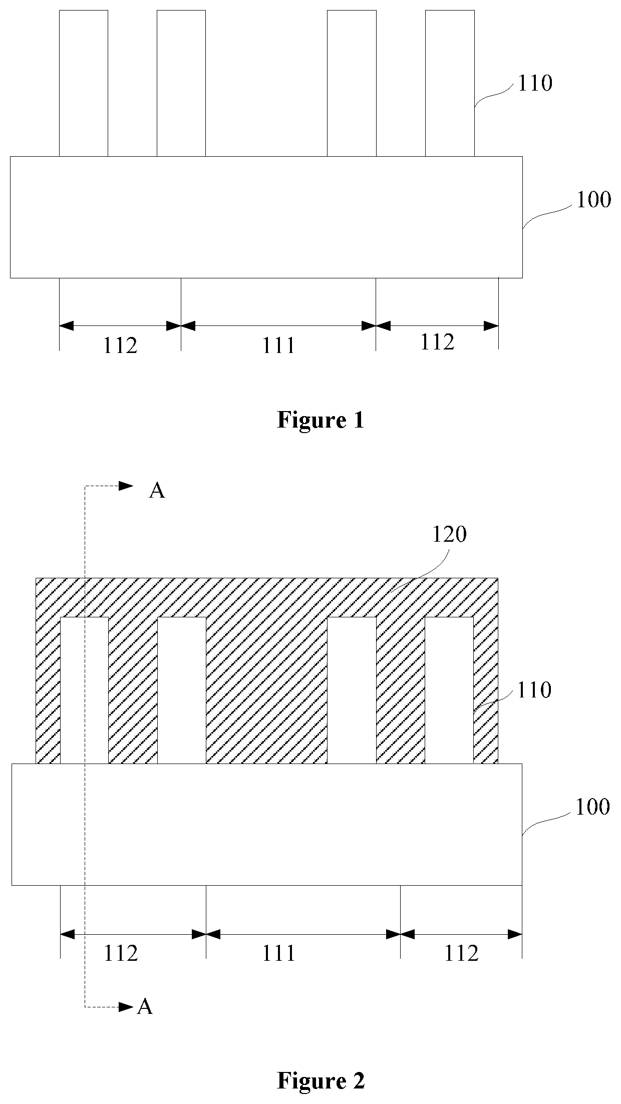
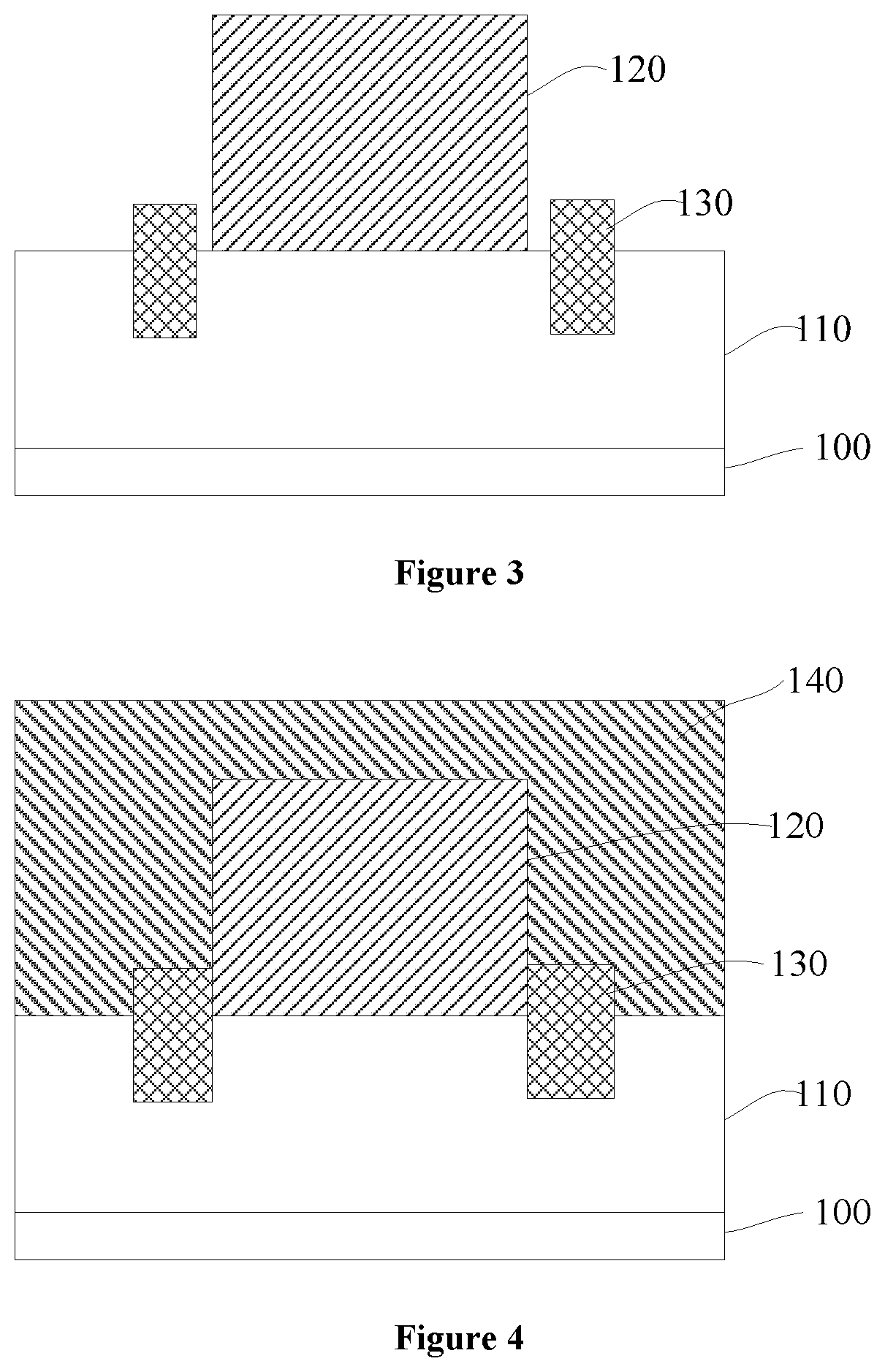
[0033]Referring to FIG. 1, a substrate 100 is provided, and a plurality of fins 110 are formed on the substrate 100. The substrate includes a fin sparse region 111 and a fin dense region 112.

[0034]Referring to FIG. 2, a gate structure 120 across a length portion of the fin 110 is formed over the substrate 100.

[0035]FIG. 3 illustrates a schematic A-A sectional ...


PUM

PropertyMeasurementUnit
temperatureaaaaaaaaaa
adhesionaaaaaaaaaa

Abstract

A semiconductor device and a method for forming the semiconductor device are provided. The method includes providing a substrate; forming a fin on the substrate, where the substrate includes a fin dense region and a fin sparse region; forming a gate structure across the fin over the substrate; forming a source-drain doped layer in the fin on both sides of the gate structure; forming a dielectric layer over the substrate, where the dielectric layer covers a top of the gate structure; and forming a first through-hole in the dielectric layer on a side of the gate structure in the fin sparse region, where a bottom of the first through-hole exposes a top sidewall of the gate structure.

Description

CROSS-REFERENCES TO RELATED APPLICATIONS[0001]This application claims the priority of Chinese patent application No. 201910899412.6, filed on Sep. 23, 2019, the entirety of which is incorporated herein by reference.FIELD OF THE DISCLOSURE[0002]The present disclosure generally relates to the field of semiconductor manufacturing technology and, more particularly, relates to a semiconductor device and a fabrication method thereof.BACKGROUND[0003]With rapid development of semiconductor manufacturing technology, semiconductor devices have been developing towards higher component density and higher degree of integration. As the most basic semiconductor devices, transistors are currently being widely used. In order to adapt to a smaller critical dimension, a channel length of a traditional planar metal-oxide-semiconductor field-effect transistor (MOSFET) is also increasingly smaller. However, as a channel length of a device keeps shrinking, the channel control capability of a gate structur...

Claims


Application Information

Patent Timeline
Patent Type & Authority Patents(United States)
IPC IPC(8): H01L21/768H01L21/311H01L29/417H01L29/66H01L29/78H01L21/285H01L29/45
CPCH01L29/41791H01L21/28568H01L21/31111H01L21/31116H01L21/31144H01L29/45H01L29/66795H01L29/7851H01L29/785H01L29/0642H01L21/76897H01L21/76895H01L21/823431H01L27/0886
Inventor WANG, NAN
Owner SEMICON MFG INT (SHANGHAI) CORP
Why Eureka
Try Eureka