Semiconductor structure and fabrication method thereof

a technology of semiconductors and semiconductor layers, applied in the direction of semiconductor devices, semiconductor/solid-state device details, electrical apparatus, etc., can solve the problems of poor performance of the existing semiconductor structure, reduce parasitic capacitance between the adjacent first interconnection layer and the second interconnection layer, reduce the rc delay, reduce the parasitic capacitance generated between the first interconnection layer and the adjacent first region, etc.

Pending Publication Date: 2021-10-07
SEMICON MFG INT (SHANGHAI) CORP +1
View PDF2 Cites 0 Cited by
  • Summary
  • Abstract
  • Description
  • Claims
  • Application Information

AI Technical Summary

Benefits of technology

[0025]The disclosed embodiments may have following beneficial effects. In the disclosed embodiments of the present disclosure, through the first interconnection structure and the third interconnection layer, the parasitic capacitance between the first interconnection layer and the second interconnection layer may be reduced, the parasitic capacitance generated between first interconnection layers formed over the adjacent first regions may be reduced, and the parasitic capacitance between the third interconnection layer and the first interconnection layer may be reduced.
[0026]First, the first interconnection layer may be formed over the first region, the second interconnection layer may be formed over the second region, and the length of the first interconnection layer may be greater than the length of the second interconnection layer. Thus, in the first direction, through the second interconnection layer with a substantially small length, the overlapped portion between the second interconnection layer and the first interconnection layer may be substantially small. Therefore, the parasitic capacitance between the adjacent first interconnection layer and the second interconnection layer may be reduced, thereby reducing the RC delay.
[0027]Second, the first interconnection layer may be formed over the first region, the second region may be disposed between adjacent first regions, and the spacing between the first interconnection layers formed over the adjacent first regions may increase. Therefore, the parasitic capacitance generated between the first interconnection layers formed over the adjacent first regions may be reduced, thereby reducing the RC delay.
[0028]Third, the third interconnection layer electrically interconnected with the second interconnection layer may be formed over the second region, and the spacing between the third interconnection layer and the first interconnection layer may increase. Therefore, the parasitic capacitance between the third interconnection layer and the first interconnection layer may be reduced, thereby reducing the RC delay.
[0029]Accordingly, through the first interconnection structure and the third interconnection layer, the parasitic capacitance between the electrical interconnection layers in the semiconductor structure may be reduced, and the RC delay may be reduced, thereby improving the performance of the semiconductor structure.

Problems solved by technology

However, performance of the existing semiconductor structure is still poor.

Method used


Image

  • Semiconductor structure and fabrication method thereof
  • Semiconductor structure and fabrication method thereof
  • Semiconductor structure and fabrication method thereof

Examples


Embodiment Construction

[0034]Reference will now be made in detail to exemplary embodiments of the disclosure, which are illustrated in the accompanying drawings. Wherever possible, the same reference numbers will be used throughout the drawings to refer to the same or the alike parts. It should be noted that “surface” in the present disclosure may be used to describe the relative positional relationship in space, and may not be limited to direct contact.

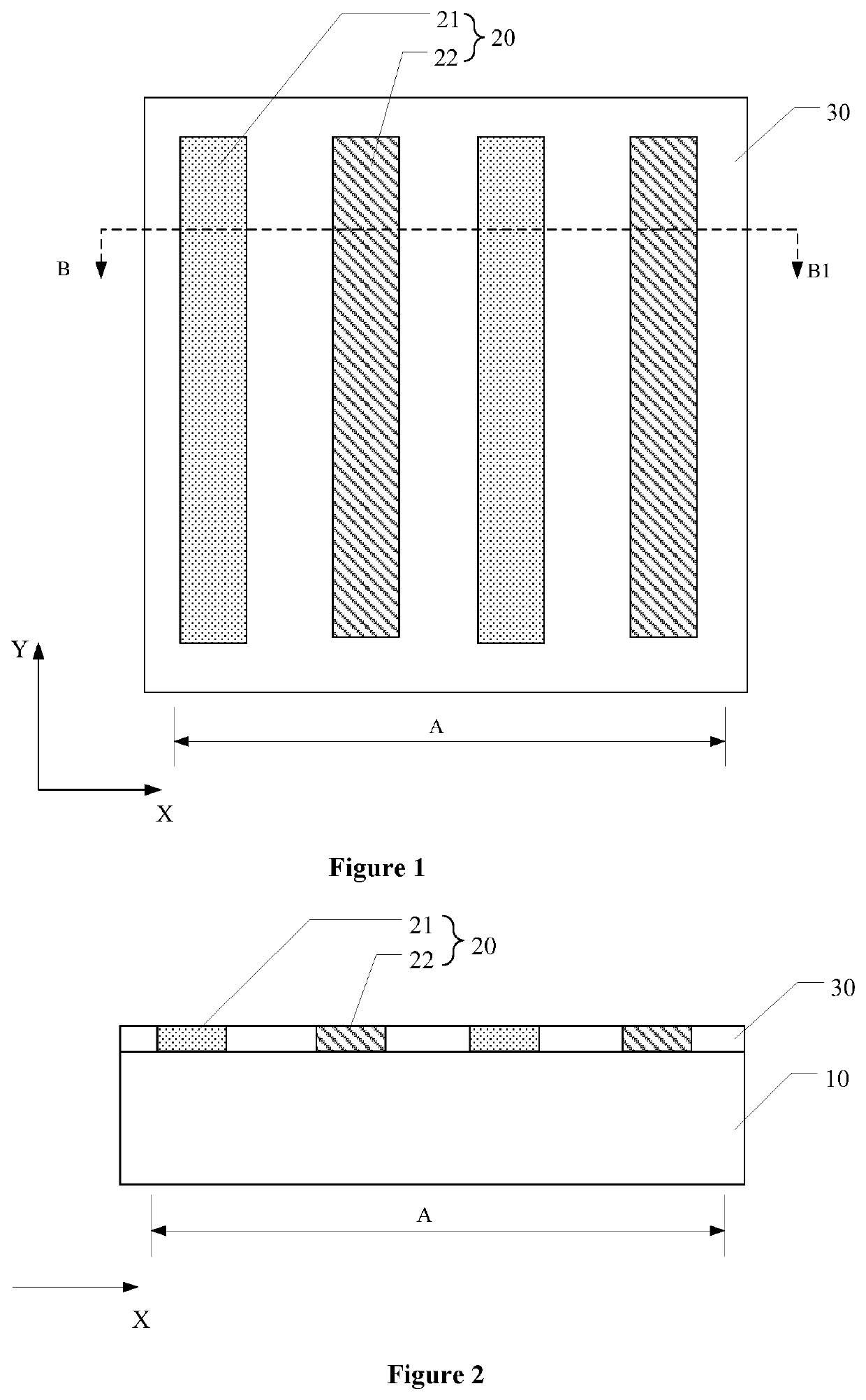
[0035]FIGS. 1-2 illustrate semiconductor structures corresponding to certain stages for forming a semiconductor structure. FIG. 1 illustrates a schematic top view of a semiconductor structure, and FIG. 2 illustrates a schematic BB1-sectional view of the semiconductor structure in FIG. 1. The semiconductor structure includes: a substrate structure 10 including a device region A, a metal interconnection layer 20 formed over the device region A, and a dielectric layer 30 surrounding the metal interconnection layer 20. The metal interconnection layer 20 includ...


PUM

PropertyMeasurementUnit
lengthaaaaaaaaaa
distanceaaaaaaaaaa
lengthaaaaaaaaaa

Abstract

A semiconductor structure and a method for forming the semiconductor structure are provided. The semiconductor structure includes a substrate structure including a device region, a first interconnection structure, and a plurality of third interconnection layers. The device region includes a plurality of first regions and one or more second regions that are arranged along a first direction. The first interconnection structure includes a plurality of first interconnection layers and a plurality of second interconnection layers that are extended along a second direction. A first interconnection layer has a length greater than a second interconnection layer in the second direction, and the first direction is perpendicular to the second direction. A third interconnection layer is disposed over the second region, and the third interconnection layer is electrically interconnected with the second interconnection layer. The third interconnection layer has a length greater than the second interconnection layer in the second direction.

Description

CROSS-REFERENCES TO RELATED APPLICATIONS[0001]This application claims the priority of Chinese patent application No. 202010252539.1, filed on Apr. 1, 2020, the entirety of which is incorporated herein by reference.FIELD OF THE DISCLOSURE[0002]The present disclosure generally relates to the field of semiconductor manufacturing technology and, more particularly, relates to a semiconductor structure and a fabrication method thereof.BACKGROUND[0003]With the continuous progress of semiconductor integrated circuit manufacturing technology, the continuous improvement of performance is also accompanied by the process of miniaturization of devices. More and more advanced manufacturing processes require the realization of as many devices as possible in a substantially small area.[0004]In an ultra-large-scale integrated circuit, the use of a metal interconnection layer is one of methods for achieving electrical interconnection between devices. However, performance of the existing semiconductor...

Claims


Application Information

Patent Timeline
Patent Type & Authority Applications(United States)
IPC IPC(8): H01L23/528H01L21/768H01L23/00
CPCH01L23/528H01L24/13H01L21/768H01L21/76847H01L21/76831H01L23/5283H01L23/5221H01L23/5222
Inventor LI, ZHI LIN
Owner SEMICON MFG INT (SHANGHAI) CORP
Why Eureka
Try Eureka