Touch panel and method of forming the same

a technology of touch panel and capacitive panel, which is applied in the field of touch panel, can solve the problems of low light transmittance, poor stability of capacitive panel, and low brightness and contras

Inactive Publication Date: 2014-09-04
CHUNG HUA UNIVERSITY
View PDF25 Cites 23 Cited by
  • Summary
  • Abstract
  • Description
  • Claims
  • Application Information

AI Technical Summary

Problems solved by technology

However, because they are bulky and inconvenient to carry, a touch input device that can be combined with a screen is additionally being developed.
A resistive type panel has a disadvantage of having low light transmittance; therefore, its brightness and contrast are low.
A capacitive panel is easily affected by panel temperature and humidity, and its detection result varies with the ground voltage level; therefore, the capacitive panel has poorer stability.
In addition, a capacitive panel cannot have a detection result if a nonconductor is used to operate.
The resolution of an optical touch panel is determined by the number of infrared emitters and corresponding receivers applied on the optical touch panel; therefore, the resolution of an optical touch panel is restricted.
Since sound waves are quite fast, a high speed signal processor and high performance analog / digital converter is required and results in high cost.
However, lowering the cost will compromise the resolution.
The present touch panels still have several disadvantages and require further improvements.

Method used


Image

  • Touch panel and method of forming the same
  • Touch panel and method of forming the same
  • Touch panel and method of forming the same

Examples


Embodiment Construction

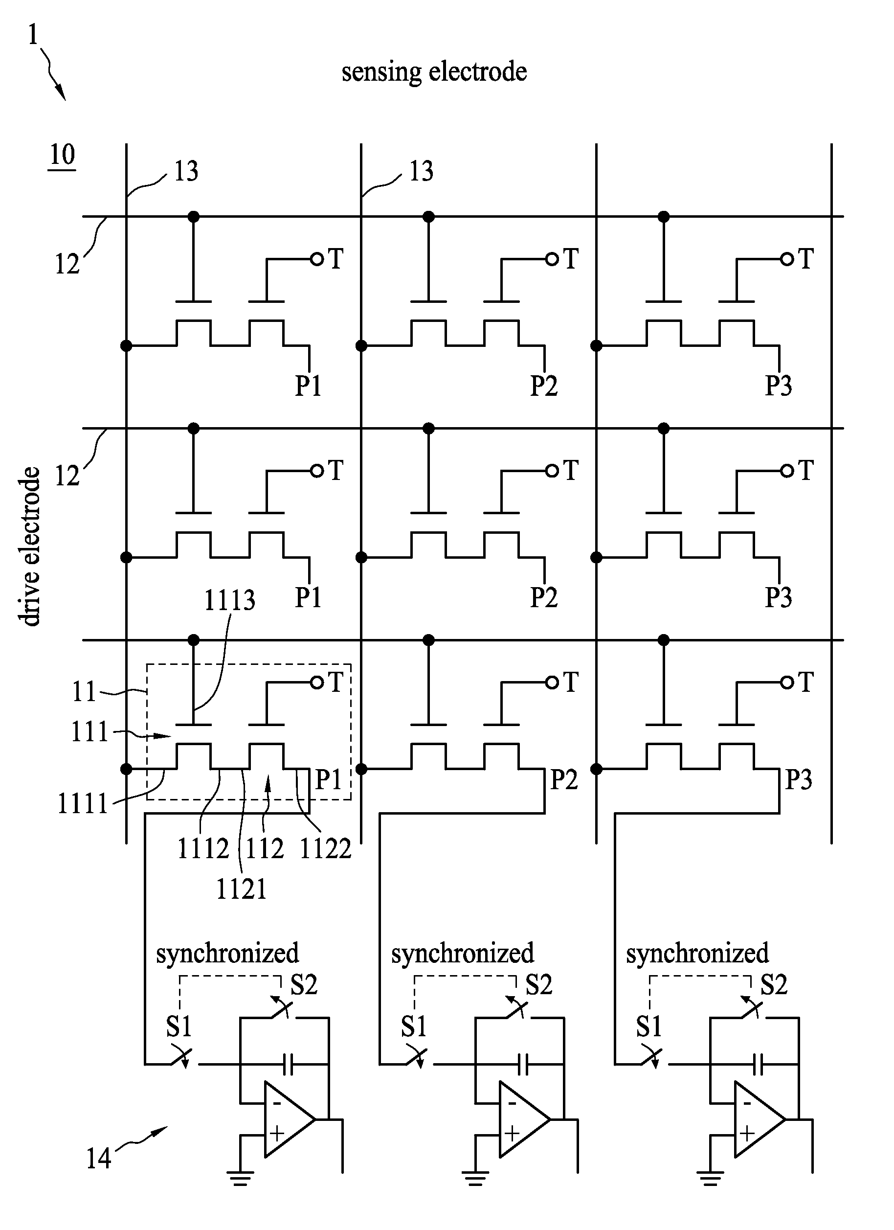
[0019]FIG. 1 schematically shows a touch panel 1 according to one embodiment of the present invention. Referring to FIG. 1, the touch panel 1 comprises a plurality of basic sensing-units 11 arrayed in a matrix. The plurality of basic sensing-units 11 can be arranged, but is not limited to being, on a substrate 10. A plurality of drive electrodes 12 and a plurality of sensing electrodes 13 are formed on the substrate 10 and separate the sensing-units 11. Each sensing-unit 11 connects to an adjacent drive electrode 12 and an adjacent sensing electrode 13. The sensing unit 11 is configured to sense a touch position, or a single touch region or multi-touch positions (or regions). The drive electrode 12 and the sensing electrode 13 can be made of a transparent conductor, such as indium tin oxide, so that the substrate 10 is transparent. A scanning voltage can be applied to the electrodes of each of two sets of drive electrodes 12 and sensing electrodes 13 one after another so as to retri...


PUM


Abstract

A touch panel comprises a plurality of basic sensing-units arranged in a matrix. The basic sensing-unit comprises a pressure-sensing transistor and a selection transistor. The pressure-sensing transistor comprises a first terminal, a second terminal, a gate electrode, a mask layer, a channel connecting the first and second terminals, a dielectric layer formed on the channel, and a piezoelectric material deposited on the dielectric layer. The piezoelectric material may comprise PVDF, lead zirconate titanate, ZnO, BaTiO3, LiNbO3, or PbTiO3. The selection transistor comprises a first terminal, a second terminal, and a third terminal. The first terminal of the selection transistor connects to a sensing electrode of the touch panel, the second terminal of the selection transistor connects to the first terminal of the pressure sensing transistor, and the third terminal of the selection transistor is a transistor gate and connects to a drive electrode of the touch panel.

Description

BACKGROUND OF THE INVENTION[0001]1. Field of the Invention[0002]The present invention relates to a touch panel and a method of forming the same.[0003]2. Description of the Related Art[0004]Due to the popularity of computers, keyboards and optical mice, such devices have become some of the most commonly used data input apparatuses. However, because they are bulky and inconvenient to carry, a touch input device that can be combined with a screen is additionally being developed.[0005]A touch panel can be operated either directly by a finger or by a stylus. A touch panel is a humanized input device that allows contact on a specific area on a panel to input a command The trend of developing light, thin, short and small electronic products with complex functions has resulted in such electronic products having reduced space for housing additional parts; therefore, having a touch panel that occupies less space is suitable. In addition to simultaneously providing the functions of a keyboard ...

Claims


Application Information

Patent Timeline
Patent Type & Authority Applications(United States)
IPC IPC(8): G06F3/041
CPCG06F3/0414G01L1/16H10N30/302
Inventor LIN, JIUM MING
Owner CHUNG HUA UNIVERSITY
Why Eureka
Try Eureka