Integrated optical crossbar switch

a crossbar switch and optical crossbar technology, applied in optics, instruments, electrical equipment, etc., can solve the problems of small grain size, unpredictability of values, and transient unbalance of optical couplers along the affected row or column

Inactive Publication Date: 2003-12-18
SOLID STATE PHOTONIX
View PDF5 Cites 20 Cited by
  • Summary
  • Abstract
  • Description
  • Claims
  • Application Information

AI Technical Summary

Benefits of technology

0139] n.sub.eff=effective index of core
0140] .sigma.=rms sidewall roughness
0141] .kappa.=0.48 for exponential autocorrelation function (ACF)
0142] and where the loss in dB / cm is given by:
0143] Inserting the values of the above system parameters: 3 Scattering Loss (dB / cm) = 1.216 10 3[ ( nm ) 1400 ] 2 ( 22 )
0144] For example with an rms sidewall roughness a .sigma.=14 nm:

Problems solved by technology

Presently, the size of these grains are unknown, but it is believed that they will be a strong function of processing temperatures; that is, low processing temperatures will result in small grain sizes.
In general, these values are not perfectly predictable, due to variations in manufacture and material temperature dependence.
The transient pulse voltage on one row or column is insufficient to cause change of state from bar to cross or vice versa, but it can cause a transient unbalance of the optical couplers along the affected row or column.
This optical coupler unbalance will create appreciable insertion loss and reflections in that column, which will introduce bit errors and decrease signal-to-noise ratio.

Method used


Image

  • Integrated optical crossbar switch
  • Integrated optical crossbar switch
  • Integrated optical crossbar switch

Examples


Embodiment Construction

[0026] 1. Introduction

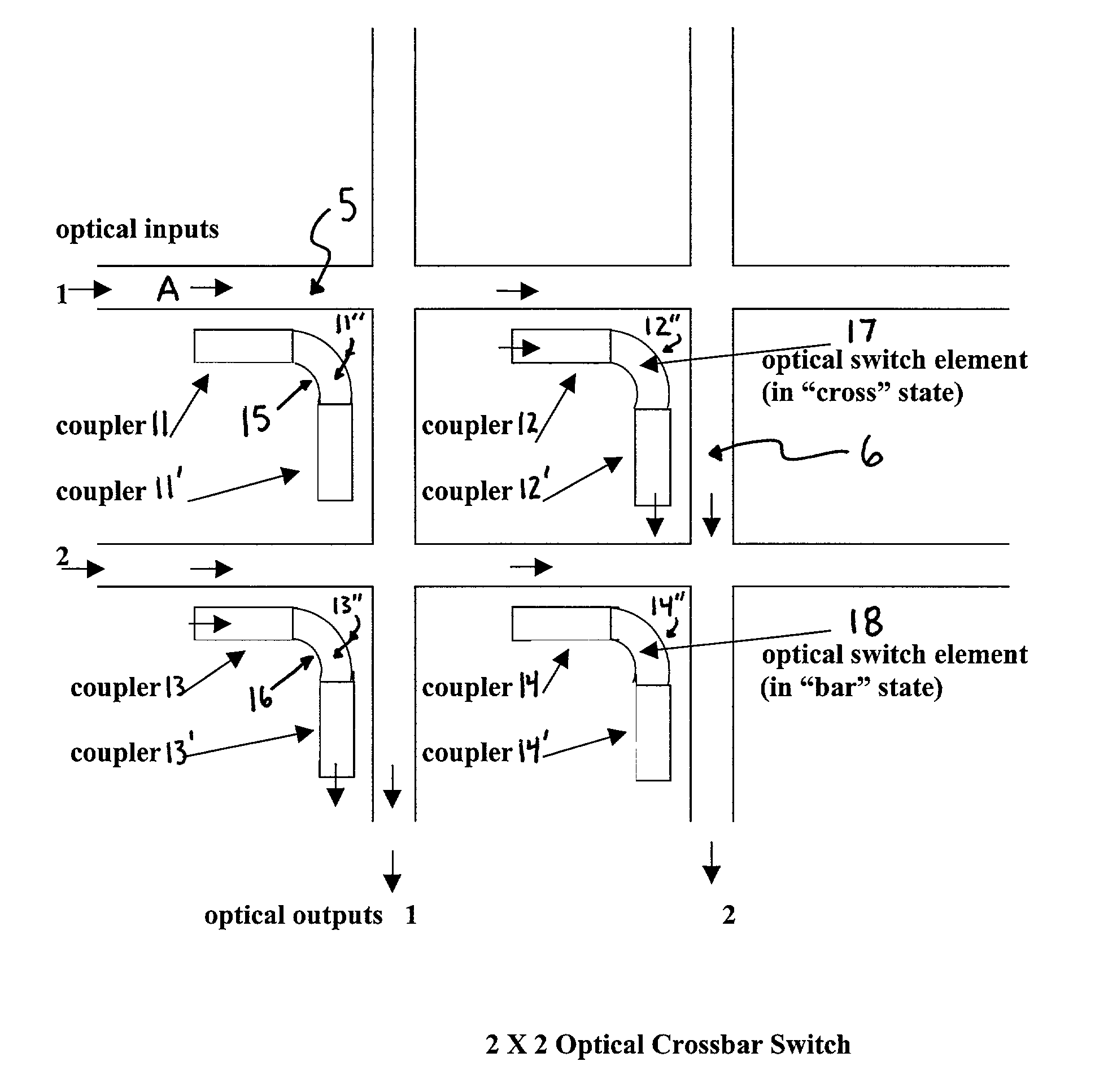
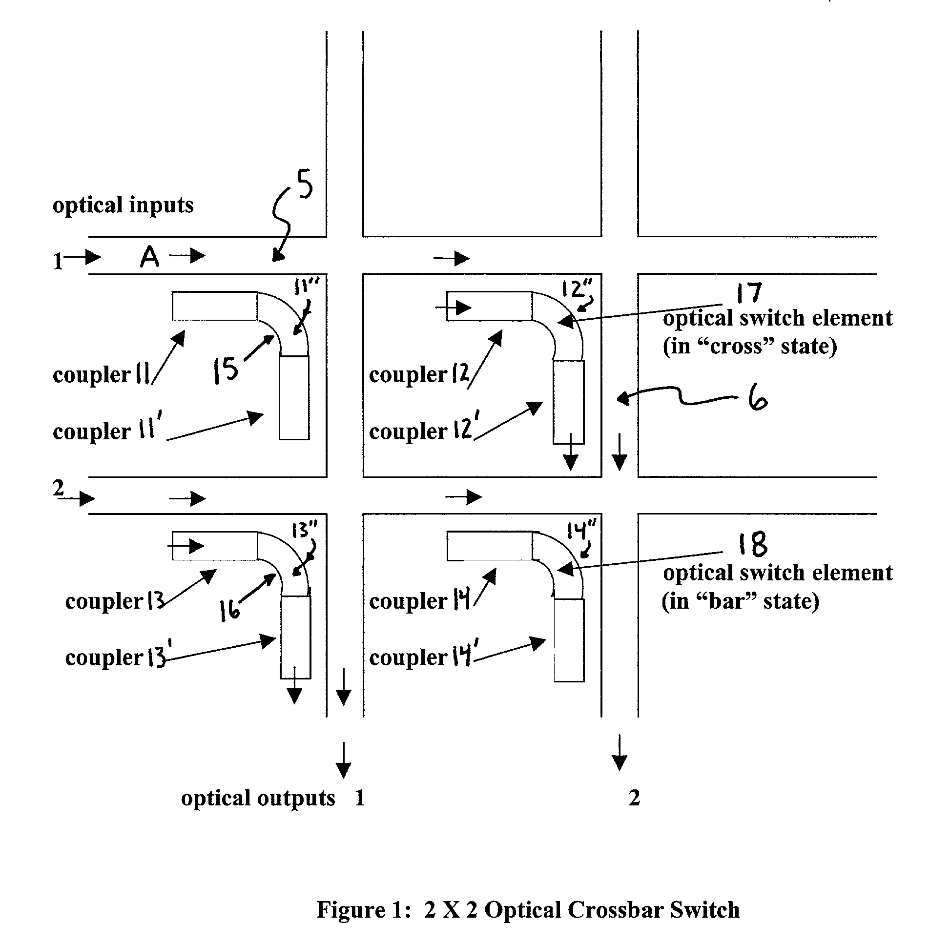
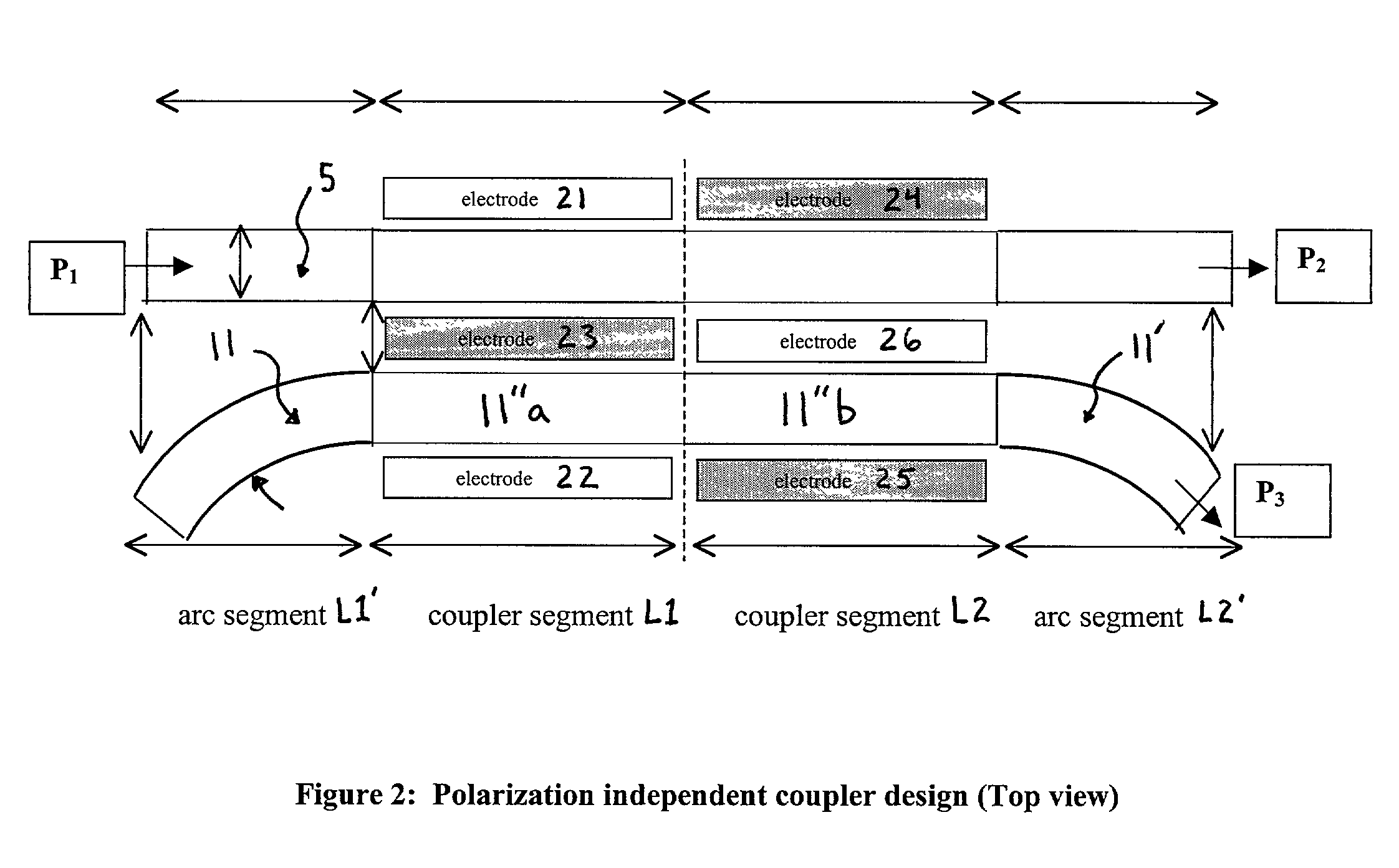
[0027] An integrated N.times.M optical crossbar switch according to the present invention preferably uses a polycrystalline ferroelectric thin film deposited on a silicon substrate. The switch can find many applications in reconfiguring optical communications systems where optical signals on optical fibers entering the switch input are directed to other optical fibers exiting the switch output. The ferroelectric material preferably is a member of the PLZT family, involving lead, lanthanum, zirconium, and oxygen, and thus has a very large electro-optical coefficient on the order of 100-400 pm / volt, both in thin film form and in bulk form. The substrate silicon provides the switching and latching function to address and maintain voltages at the selected crossbar elements. This approach results in a solid state, non-blocking optical switch with low insertion loss, low crosstalk, and polarization independence, addressable by N+M external control lines. Because of t...


PUM

PropertyMeasurementUnit
anglesaaaaaaaaaa
sizeaaaaaaaaaa
sizeaaaaaaaaaa

Abstract

Integrated optical crossbar switching method and apparatus preferably includes structure and/or function whereby switching and addressing circuitry is disposed on a substrate. An insulating layer is disposed on the substrate and on the switching and addressing circuitry. A polycrystalline ferroelectric layer is disposed on the insulating layer. The polycrystalline ferroelectric layer includes a first plurality of optical signal carriers and a second plurality of optical signal carriers, each disposed to receive an optical signal from at least one of the first plurality of optical signal carriers. A plurality of optical switching elements is disposed to (i) receive control and addressing signals from said switching and addressing circuitry, and (ii) to switch an optical signal from one of said first plurality of optical signal carriers to at least one of said second plurality of optical signal carriers. Preferably, PLZT (lead lanthanum zirconate titanate) materials are used in the core and cladding of the optical switching elements.

Description

[0001] 1. Field of the Invention[0002] The present invention relates to optical crossbar switching method and apparatus.[0003] 2. Related Art[0004] Optical switches in optical communications systems can reconfigure a fiber optic network on the order of a millisecond or less. These all-optical switches (OOO) imply that the input signal is optical, the output signal is optical and the switching action occurs in the optical domain. This is to be contrasted with the more common OEO switches where the input signal is optical, the output signal is optical and the signal is controlled in the electrical domain. An OOO switch is said to be transparent to the optical signals sent through the switch. For example, any kind of modulation scheme can be used (analog or digital), any bitrate, and any type of format can be superimposed and transmitted without interfering with one another and without their information being modified within the network. This is to be contrasted with the OEO switch, wh...

Claims


Application Information

Patent Timeline
Patent Type & Authority Applications(United States)
IPC IPC(8): G02F1/055G02F1/313H04Q11/00
CPCG02F1/0553G02F1/3132H04Q2011/0058H04Q2011/0024H04Q2011/0039H04Q11/0005
Inventor CLARKE, WILLIAM L.LEVINE, JULES D.
Owner SOLID STATE PHOTONIX
Why Eureka
Try Eureka