Display device

a display device and substrate technology, applied in the field of display devices, can solve the problems of substrate or a wiring provided over the substrate being destroyed, connection wiring peeling from the substrate, etc., and achieve the effect of high-reliability display devices

Active Publication Date: 2014-09-11
SEMICON ENERGY LAB CO LTD
View PDF3 Cites 184 Cited by
  • Summary
  • Abstract
  • Description
  • Claims
  • Application Information

AI Technical Summary

Benefits of technology

[0008]An object of one embodiment of the present invention is to provide a highly reliable display device. In particular, an object is to provide a display device to which a signal or a power supply potential can be supplied stably. Further, an object is to provide a bendable display device to which a signal or a power supply potential can be supplied stably.
[0018]With one embodiment of the present invention, a highly reliable display device can be provided. Further, a display device to which a signal or a power supply potential can be supplied stably can be provided. Further, a bendable display device to which a signal or a power supply potential can be supplied stably can be provided.

Problems solved by technology

However, a display device including a display element over a flexible substrate has a problem in that the substrate or a wiring provided over the substrate may be destroyed by heat or pressure applied by thermocompression bonding.
Further, the display device also has a problem in that the connection wiring peels from the substrate by curving the substrate.

Method used


Image

  • Display device
  • Display device
  • Display device

Examples


embodiment 1

[0035]In this embodiment, configuration examples of a display device of one embodiment of the present invention will be described with reference to drawings.

[Configuration Example of Display Device]

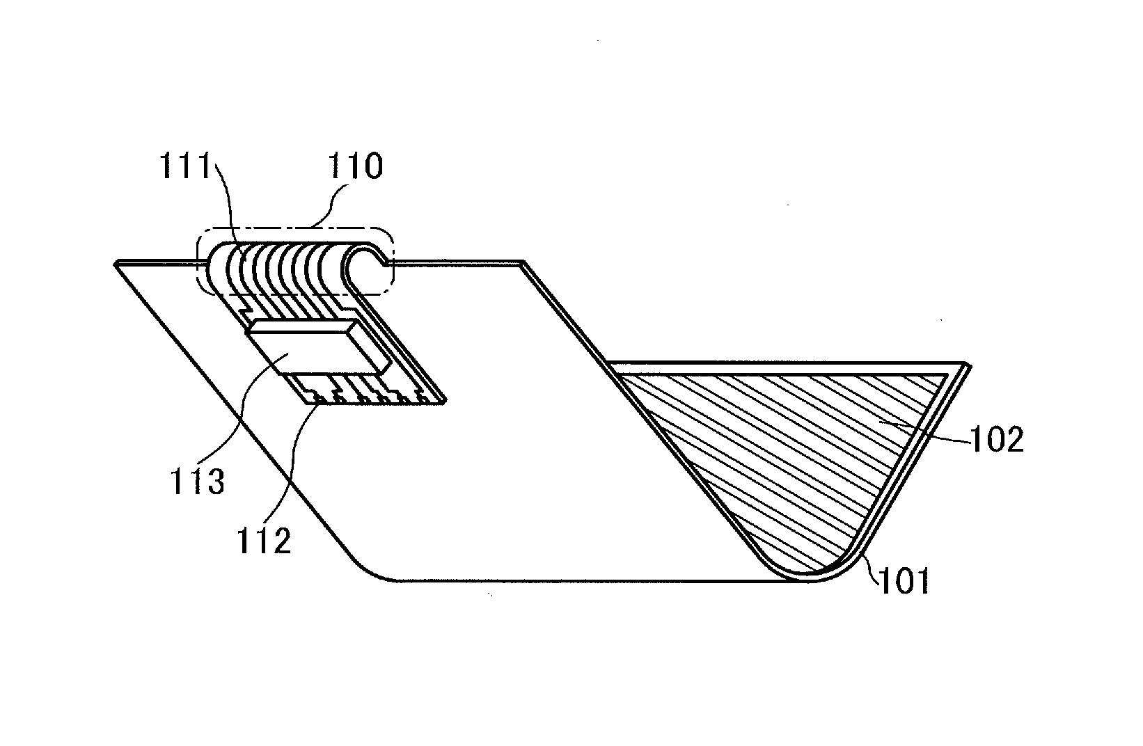
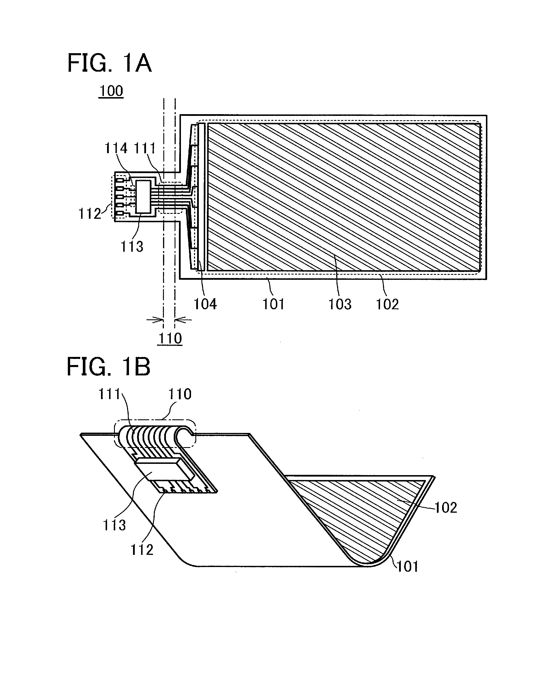
[0036]FIG. 1A is a schematic top view of a display device 100 of one embodiment of the present invention.

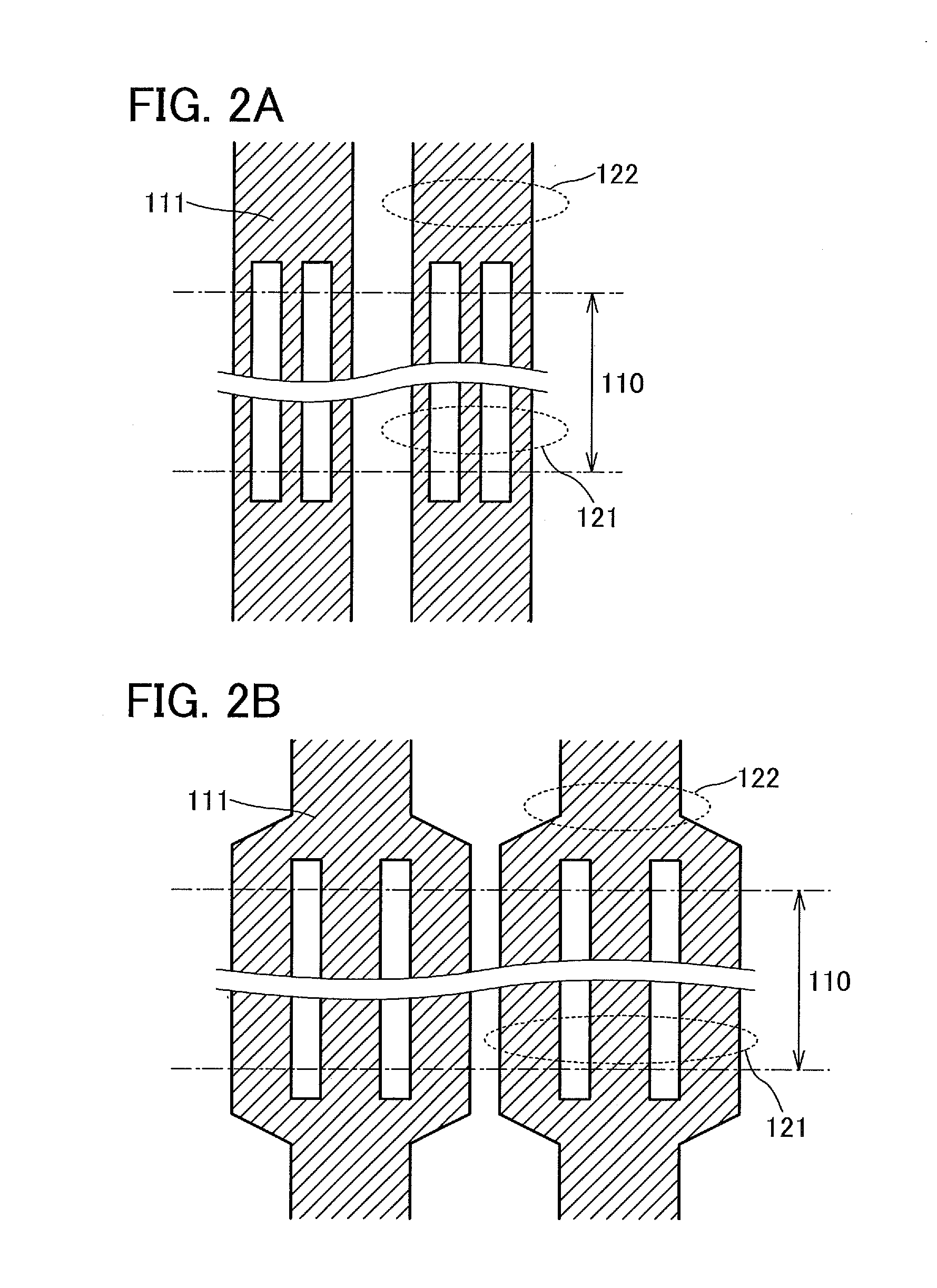
[0037]The display device 100 includes a display portion 102, a plurality of wirings 111, a plurality of connection terminals 112, an IC 113, and a plurality of wirings 114 over a flexible substrate 101.

[0038]The display portion 102 includes a pixel portion 103 and a driver circuit 104.

[0039]In the pixel portion 103, pixels each including a display element are arranged in a matrix. By driving each pixel, an image can be displayed on the pixel portion 103.

[0040]As a display element that can be used in a pixel, an organic electroluminescence (EL) element, a liquid crystal element, or the like can be used. Alternatively, an element that performs display by an electrophoretic method, an ele...

embodiment 2

[0115]An example of a method for manufacturing a display device of one embodiment of the present invention will be described below.

[Example of Manufacturing Method]

[0116]First, a separation layer 202 is formed over a supporting substrate 201.

[0117]As the supporting substrate 201, a substrate having heat resistance to at least the heat applied in a subsequent process is used. Examples of the supporting substrate 201 include a glass substrate, a resin substrate, a semiconductor substrate, a metal substrate, and a ceramic substrate.

[0118]As a material of the separation layer 202, a high melting point metal material such as tungsten, titanium, or molybdenum can be used, for example. Tungsten is preferably used.

[0119]The separation layer 202 can be formed by a sputtering method, for example.

[0120]Then, a separation layer 203 is formed over the separation layer 202. An oxide layer 211 is formed between the separation layer 202 and the separation layer 203.

[0121]As a material of the separa...

embodiment 3

[0165]In this embodiment, specific configuration examples of the display device described in Embodiment 1 will be described with reference to drawings. Examples of an image display device to which an organic EL element is used will be described below.

[Configuration Example 1 of Display Device]

[0166]FIG. 9 is a schematic cross-sectional view of a display device 300 with a top emission structure. The schematic top view of the display device 300 of FIG. 9 corresponds to FIG. 1A, and FIG. 9 corresponds to a schematic cross-sectional view of the region including the display portion 102, the wiring 111, and the connection terminal 112 in FIGS. 1A and 1B.

[0167]The display device 300 includes the separation layer 203 over a flexible substrate 354 with an adhesive layer 135 interposed therebetween. The display device 300 further includes, over the separation layer 203, the pixel portion 103 including a light-emitting element 340, the driver circuit 104, the wiring 111, and the connection ter...


PUM


Abstract

One embodiment of the present invention provides a highly reliable display device. In particular, a display device to which a signal or a power supply potential can be supplied stably is provided. Further, a bendable display device to which a signal or a power supply potential can be supplied stably is provided. The display device includes, over a flexible substrate, a display portion, a plurality of connection terminals to which a signal from an outside can be input, and a plurality of wirings. One of the plurality of wirings electrically connects one of the plurality of connection terminals to the display portion. The one of the plurality of wirings includes a first portion including a plurality of separate lines and a second portion in which the plurality of lines converge.

Description

TECHNICAL FIELD[0001]The present invention relates to a display device. In particular, one embodiment of the present invention relates to a display device including a bendable display portion.BACKGROUND ART[0002]In recent years, diversification of the shape of electronic devices having a display function has been required. For example, an electronic device including a display device in which a display element is provided over a flexible substrate that is bendable and can display images on the curved surface is demanded. This display device is also called a flexible display and is under development for practical application.[0003]An organic electroluminescence (EL) element, a liquid crystal element, or the like can be used as a display element for flexible displays. The flexible display is, for example, an electronic paper including an element that performs display by an electrophoretic method or an electronic liquid powder method.[0004]For example, Patent Document 1 discloses an org...

Claims


Application Information

Patent Timeline
Patent Type & Authority Applications(United States)
IPC IPC(8): H05K7/06H05B44/00
CPCH05K7/06H10K59/131H10K77/111H10K2102/311Y02E10/549H10K59/1213H10K71/00H05K1/0277H05K1/028H05K1/0283H05K1/189H05K2201/05H05K1/147H05K2201/051H05K2201/053H05K2201/055H05K2201/052H10K59/1201G04G9/0088H01L27/1244
Inventor YAMAZAKI, SHUNPEIYOSHIZUMI, KENSUKE
Owner SEMICON ENERGY LAB CO LTD
Why Eureka
Try Eureka