

Observation specimen for use in electron microscopy, electron microscopy, electron microscope, and device for producing observation specimen
- Summary
- Abstract
- Description
- Claims
- Application Information
AI Technical Summary
Benefits of technology
Problems solved by technology
Method used
Image

Examples
first embodiment
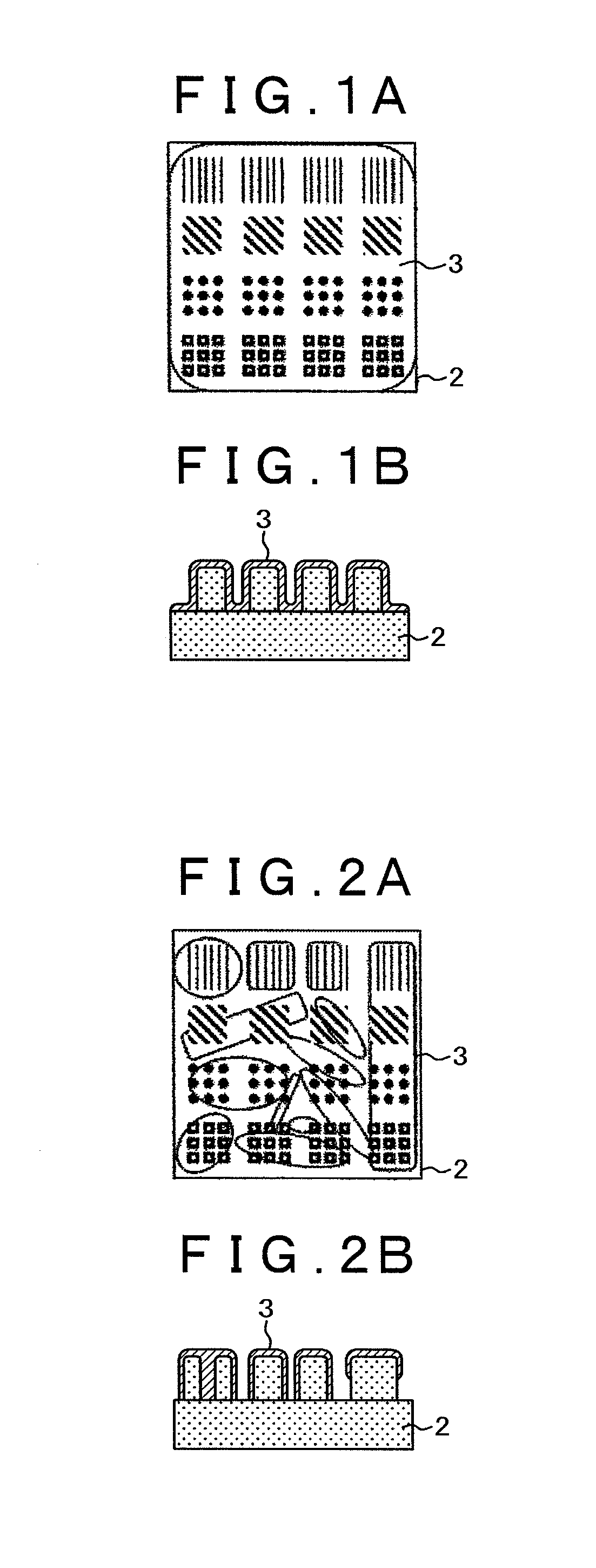
[0053]FIG. 1A is a top view of an observation specimen that a liquid medium including an ionic liquid on a sample is in a thin film shape, and FIG. 1B is a cross sectional view of the observation specimen that the liquid medium including an ionic liquid is in a thin film shape. A sample 2 is a sample including groove patterns, and a liquid medium 3 including an ionic liquid is an ionic liquid in a thin film shape on the groove patterns. In the embodiment, an electron microscopic method will be described using the observation specimen that the liquid medium including an ionic liquid on the sample is in a thin film shape as illustrated in FIG. 1. It is noted that the ionic liquid for use in the present invention is 1-Butyl-3-methylimidazolium Tetrafluoroborate, 1-Ethyl-3-methylimidazolium bis (trifluoromethylsulfonyl) imide, and 1-Butyl-3-methylimidazolium bis (trifluoromethylsulfonyl) imide, for example. In the embodiment, a liquid medium including an ionic liquid was used in which t...
second embodiment
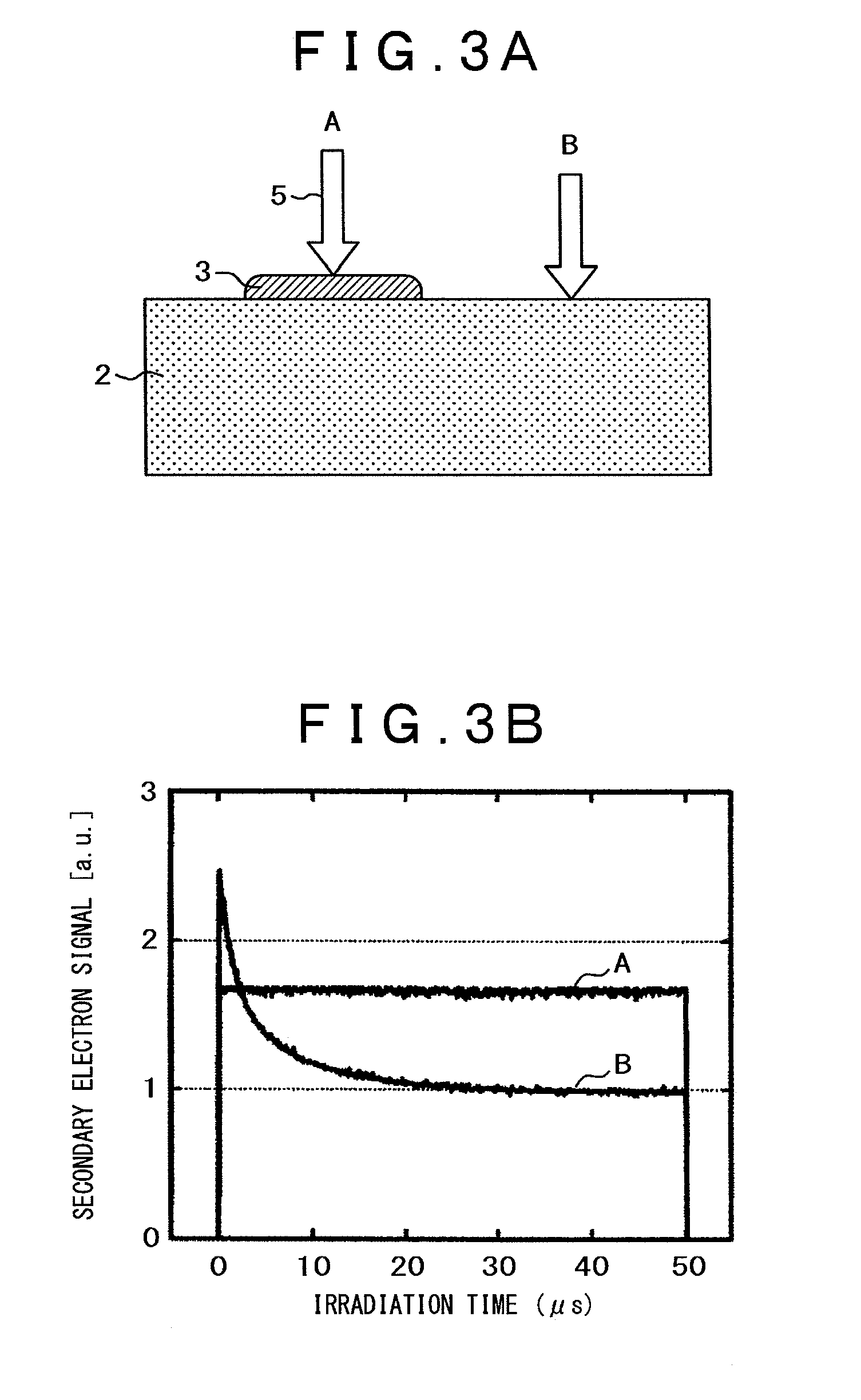
[0059]In this embodiment, an electron microscopic method will be described in which the film thickness of an ionic liquid is measured and the irradiation conditions for the primary electrons are controlled based on the measured film thickness. In the embodiment, the observation specimen was used that the ionic liquid on the sample is in a thin film shape in C in FIG. 5A shown in the first embodiment.
[0060]In consideration of the film thickness of the ionic liquid and the range of low-energy primary electrons, the irradiation conditions for the primary electrons are controlled. Here, the range of electrons means the length of electrons passing through the inside of a substance. As described in a reference (K. Kanaya, S. Okayama, J. Phys. D. Appl. Phys. 5, 43 (1972)), a range R (μm) of the primary electrons is expressed by Equation 1.
R=0.0276(eV)5 / 3Aρ8 / 9Z[Equation1]
[0061]ρ (g / cm3) is the density of a substance through which electrons pass, Z is an atomic number, A (g / mol) is an atomic...
third embodiment
[0072]In the embodiment, an electron microscopic method will be described using an observation specimen in which an ionic liquid is applied to a sample and then formed into a thin film. In the embodiment, a resist sample having line groove patterns was used.
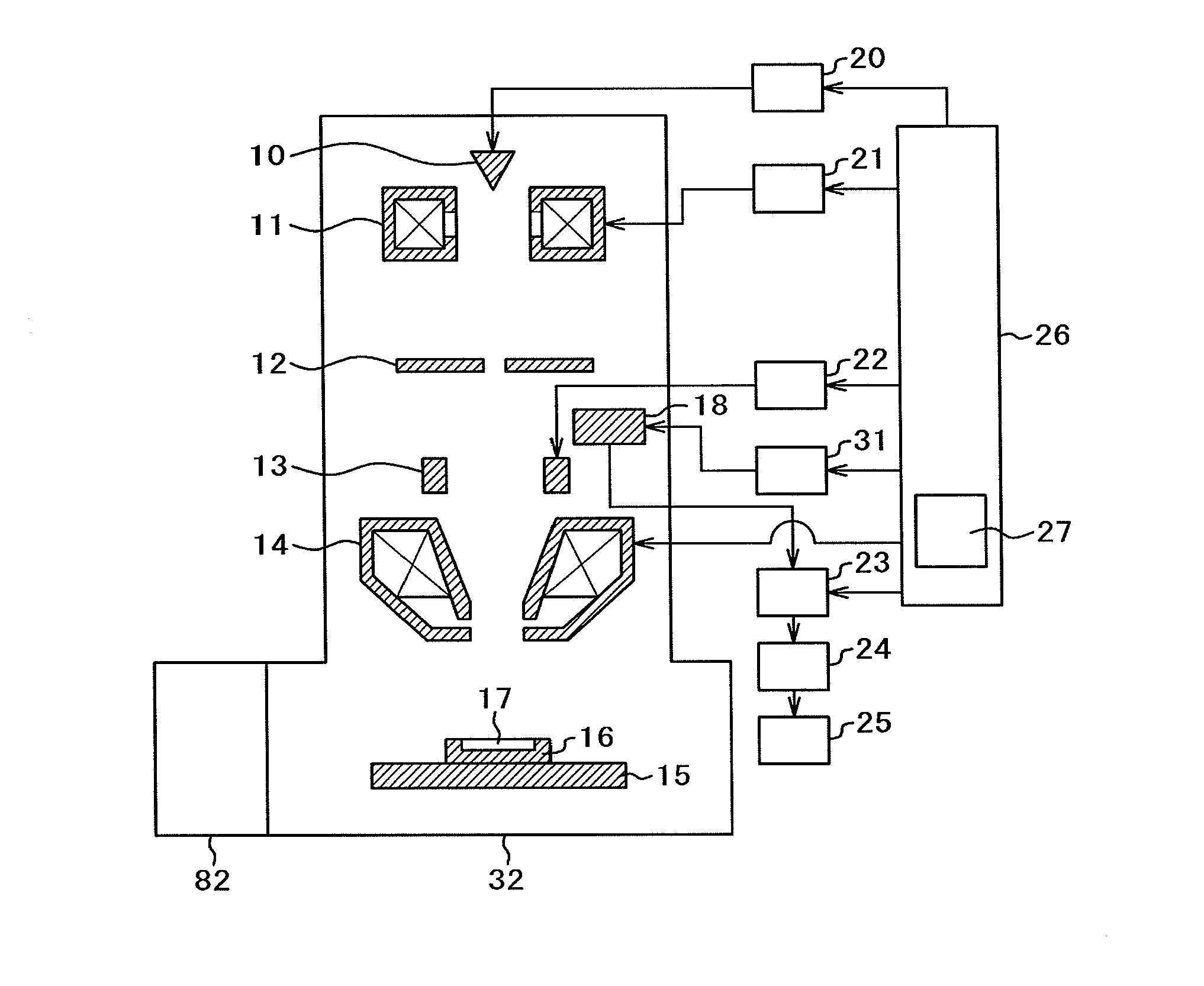
[0073]FIG. 10 is a block diagram of an observation specimen preparation device for an electron microscopic method according to the embodiment. Here, the observation specimen preparation device is a device that applies an ionic liquid to a sample and prepares an observation specimen, including an ionic liquid adjusting unit 72 that mixes an ionic liquid with a substance different from the ionic liquid, an ionic liquid discharging unit 73, a sample 74, a sample holder 75, a sample holding unit 76, a sample holding unit rotating mechanism 77, a valve 80, an exhaust mechanism 81, an exhaust chamber 82, and a control system. The control system is configured of an ionic liquid adjustment control unit 84, a discharge control unit 85, a ...
PUM
 Abstract
Description
Claims
Application Information