Method for fabricating semiconductor device

a semiconductor and device technology, applied in the direction of semiconductor devices, basic electric elements, electrical equipment, etc., can solve the problems of high cost, high cost, and high defect rate of thin film transistors, and achieve the effects of low carrier mobility and low current, and high cos

Inactive Publication Date: 2014-09-25
NAT CHIAO TUNG UNIV
View PDF1 Cites 12 Cited by
  • Summary
  • Abstract
  • Description
  • Claims
  • Application Information

AI Technical Summary

Benefits of technology

[0015]Therefore, the advantage and spirit of the present invention can be understood further by the following detail description of invention and attached Figures.

Problems solved by technology

However, abovementioned technology and material have had many problems all the time, which face the bottleneck on the technological break-through.
Firstly, based on the process of thin film transistor at present, there are often a lot of defects in the thin film transistor.
The existence of these defects will cause low carrier mobility and low current.
At the same time, they can cause high leakage current of device and reduce the reliability device.
However, as for the abovementioned conventional furnace tube annealing process, the high-temperature, long-term process not only will cause the damage of device, but also will increase the burden of process.

Method used


Image

  • Method for fabricating semiconductor device
  • Method for fabricating semiconductor device
  • Method for fabricating semiconductor device

Examples


Embodiment Construction

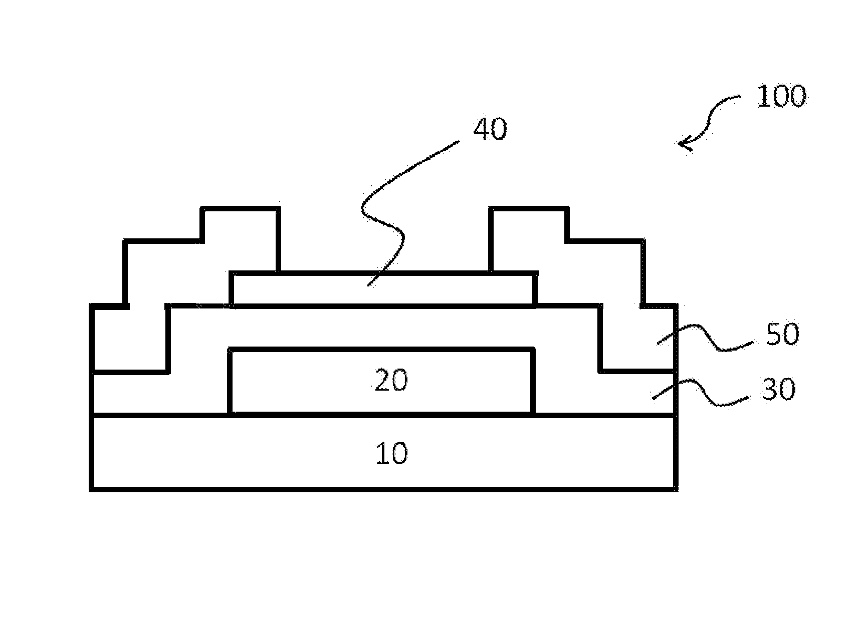
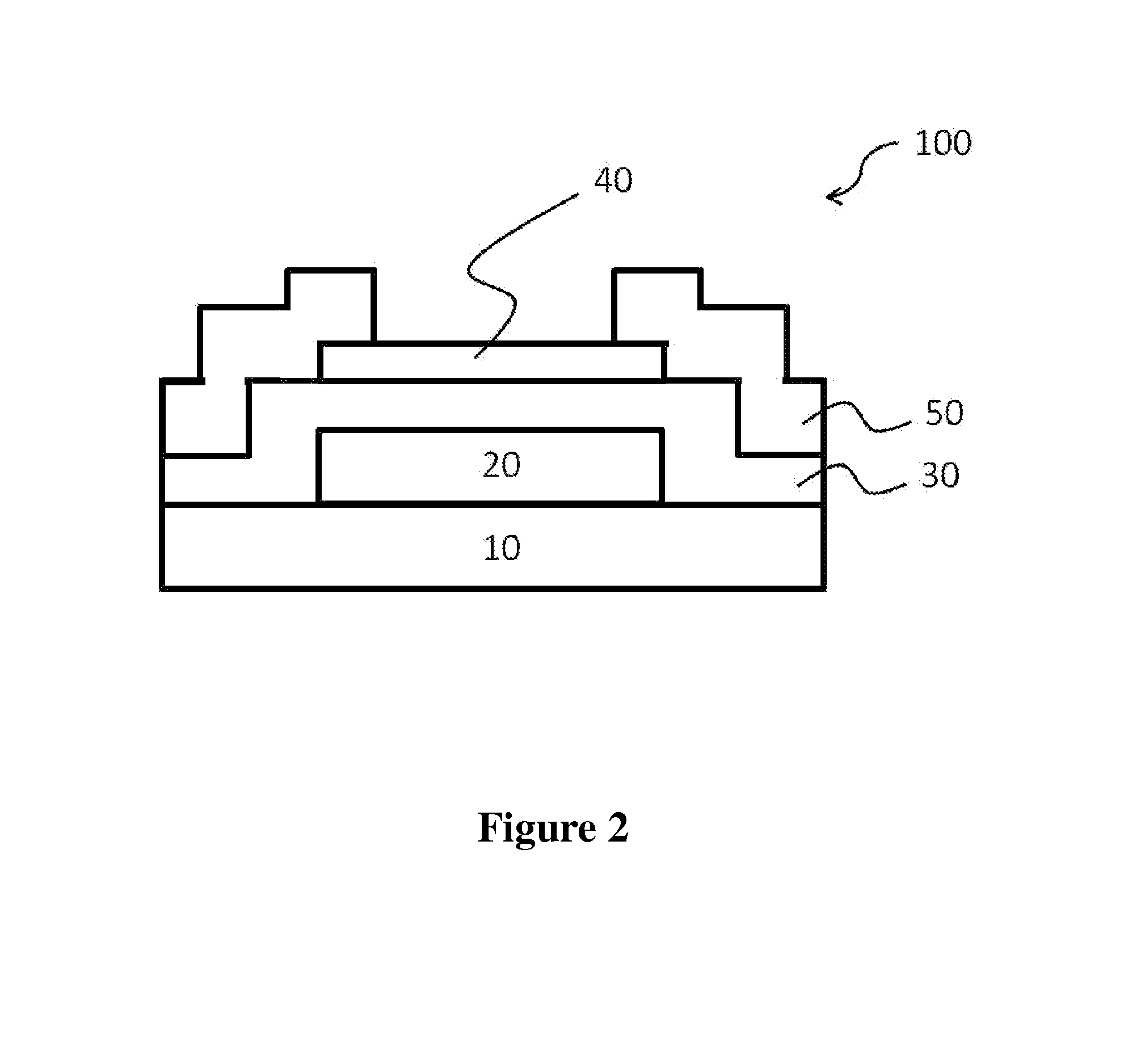
[0026]As the abovementioned description, please refer to FIG. 1 and FIG. 2. FIG. 1 illustrates the flow chart of the method for fabricating semiconductor device according to an embodiment of the present invention. FIG. 2 illustrates the side view of the semiconductor device according to an embodiment of the present invention. As shown in the

[0027]Figure, the present invention provides a method for fabricating semiconductor device, which comprises the following steps. Firstly, as shown in Step S 100, a gate 20 is formed on a substrate 10. As shown in Step S 102, a gate insulating layer 30 is then formed on the gate 20, and as shown in Step S104, an active layer 40 is further disposed on the gate insulating layer 30. As shown in Step S106 and Step S108, the source / drain 50 are defined on the active layer 40 to form the semiconductor device 100, and a microwave annealing process is finally performed thereon.

[0028]It has to describe that in the present invention, the active layer 40 is ...


PUM


Abstract

A method for fabricating a semiconductor device is disclosed in the present invention. The abovementioned method comprises the following steps. Firstly, a gate is formed on a substrate. A gate insulating layer is then formed on the gate, and further an active layer is disposed on the gate insulating layer, wherein the active layer is composed of a microwave absorbing material. Source/drain is defined on the active layer to form the semiconductor device, and a microwave annealing process is finally performed thereon.

Description

BACKGROUND OF THE INVENTION[0001]1. Field of the Invention The present invention relates to a method for fabricating semiconductor device, and particularly to a method for fabricating semiconductor device by employing a microwave annealing process to increase the efficiency and electric reliability of semiconductor device.[0002]2. Description of the Prior Art[0003]Accompanying with the flourishing development of the Flat Panel Display (FPD) technology, the application of Thin Film Transistor (TFT) has been paid great attention. At present, the thin film device has been used to substitute the external integrated circuit set, in order to produce the System on Panel (SoP) for various displays and reach the goal of light, thin, low cost and high yield. Wherein, the amorphous metal oxide semiconductor has the characteristics of high carrier mobility, low process temperature, high transmittance, excellent homogeneity and transparency, which is very suitable for applying in future relevant...

Claims


Application Information

Patent Timeline
Patent Type & Authority Applications(United States)
IPC IPC(8): H01L21/477H01L29/66
CPCH01L29/6675H01L21/477H01L29/66969H01L29/78693H01L21/02488H01L21/02554H01L21/02565H01L21/02631
Inventor LIU, PO-TSUNTENG, LI-FENGLO, YUAN-JOULEE, YAO-JEN
Owner NAT CHIAO TUNG UNIV
Why Eureka
Try Eureka