Semiconductor device

a technology of semiconductors and devices, applied in the field of semiconductor devices, can solve the problems of increasing the power consumption of cpu, difficult to stop the supply of power in a period during which the cpu does not operate, etc., and achieve the effects of reducing overhead time, reducing overhead power, and reducing power consumption

Active Publication Date: 2014-10-02
SEMICON ENERGY LAB CO LTD
View PDF4 Cites 21 Cited by
  • Summary
  • Abstract
  • Description
  • Claims
  • Application Information

AI Technical Summary

Benefits of technology

[0020]According to one embodiment of the present invention, it is possible to provide a semiconductor device capable of reducing overhead power, a semiconductor device capable of reducing overhead time, or a device achieving lower power consumption by using one of the semiconductor devices.

Problems solved by technology

In a normally-off computer, a short period of stopping the supply of power for power gating is likely to increase power consumption of a CPU when a break even time (BET) is long.
Further, in the normally-off computer, if overhead time including time required for data saving and restoration in power gating is not short, it is difficult to stop the supply of power in a period during which the CPU does not operate.

Method used


Image

  • Semiconductor device
  • Semiconductor device
  • Semiconductor device

Examples


embodiment 1

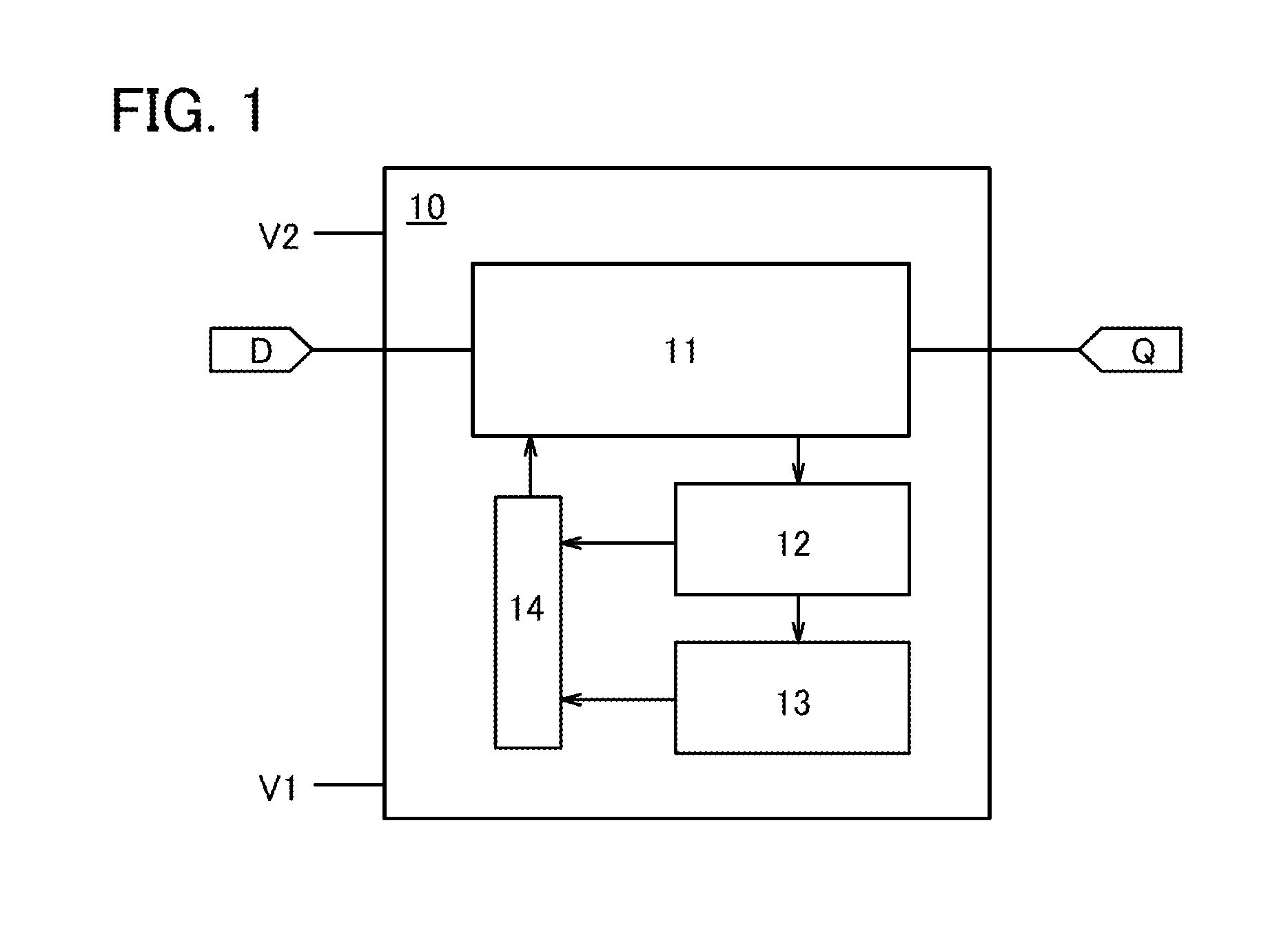
[0035]FIG. 1 illustrates an example of the structure of a semiconductor device in one embodiment of the present invention. A semiconductor device 10 illustrated in FIG. 1 includes a first memory circuit 11 (first circuit), a second memory circuit 12 (second circuit), a third memory circuit 13 (third circuit), and a read circuit 14 (fourth circuit).

[0036]As a power supply voltage, a potential difference between a potential V1 and a potential V2 is supplied to the semiconductor device 10. One of the potential V1 and the potential V2 is high, and the other is low. The following shows an example of the structure of a semiconductor device in one embodiment of the present invention when the potential V1 is low and the potential V2 is high.

[0037]The first memory circuit 11 has a function of retaining data when a signal D including the data is input in a period during which the power supply voltage is supplied to the semiconductor device 10. The first memory circuit 11 outputs a signal Q in...

embodiment 2

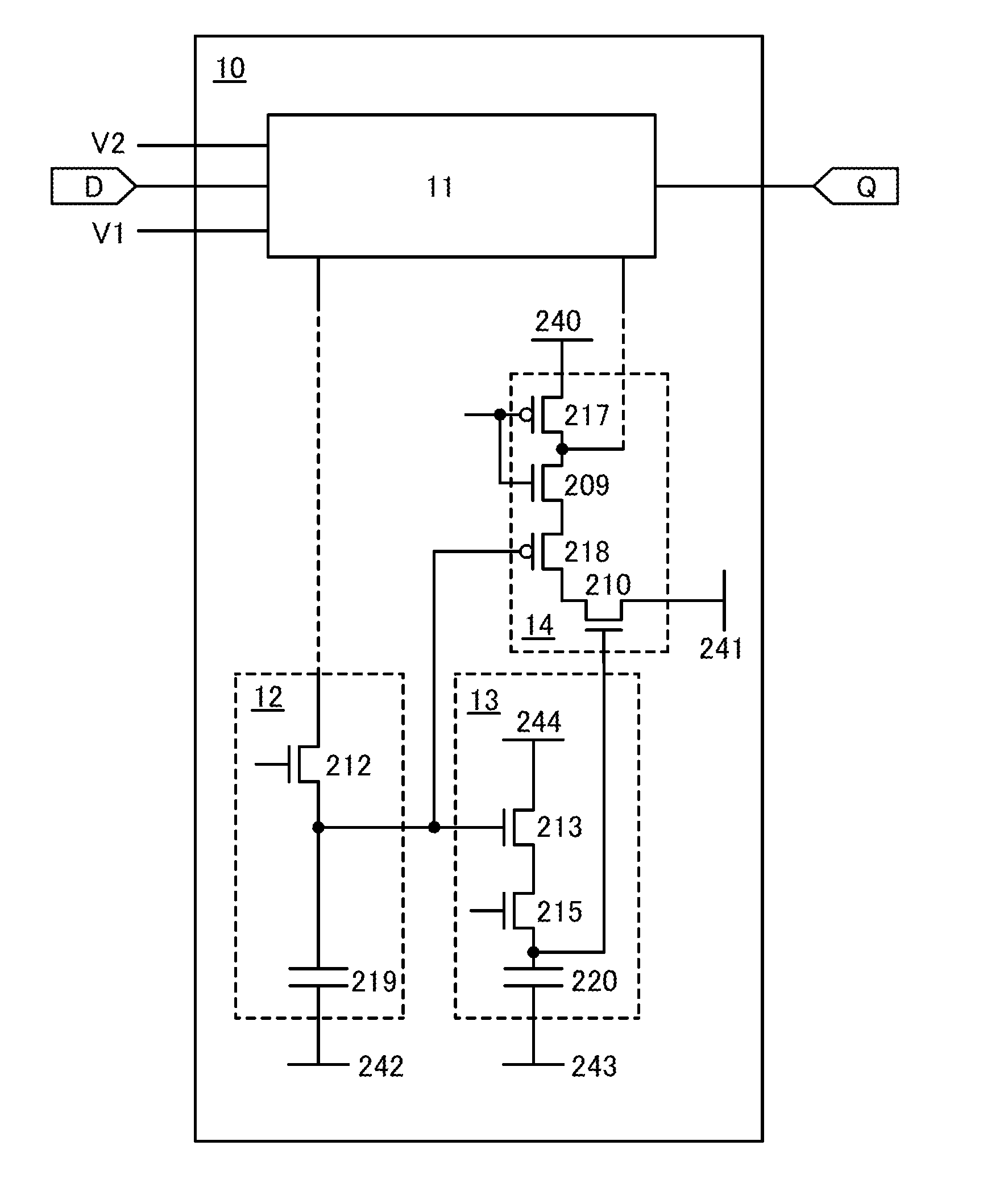
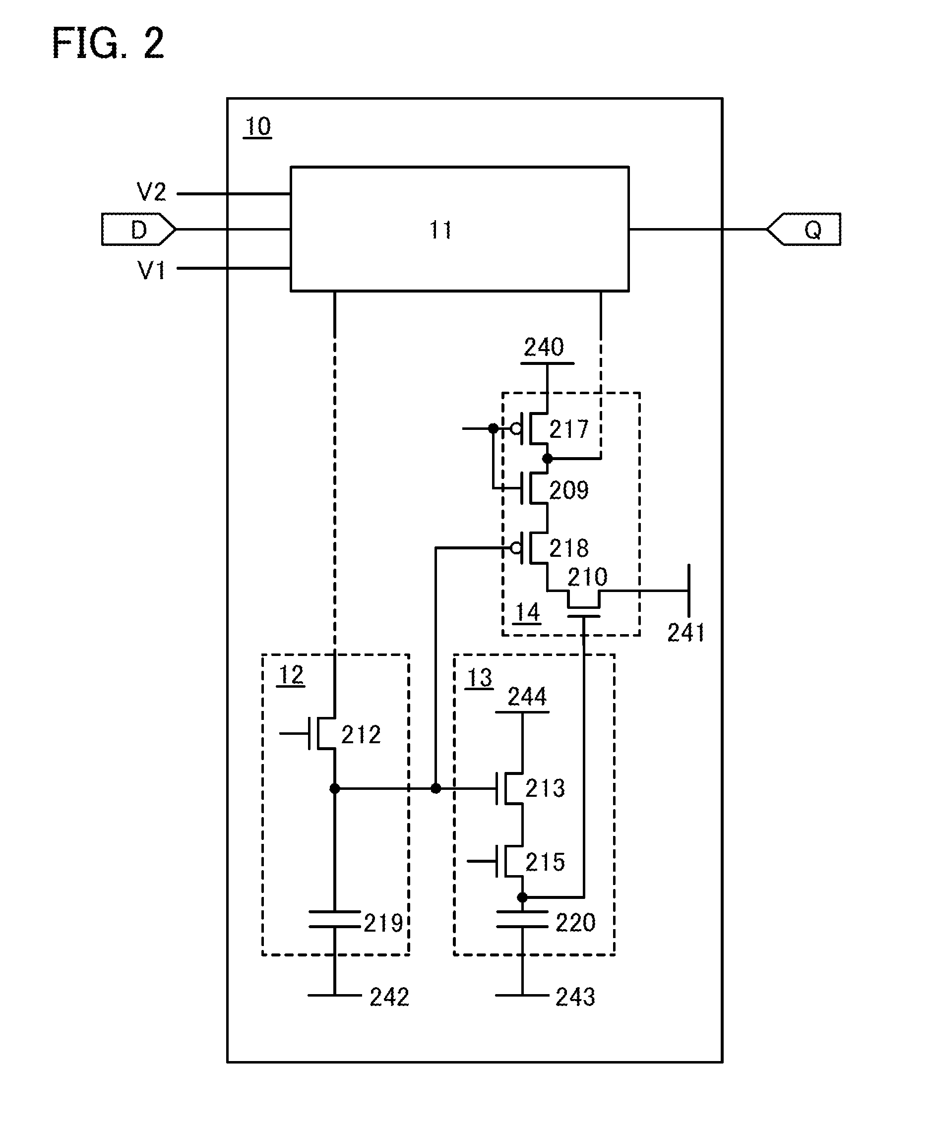
[0052]In this embodiment, an example of a specific structure of the semiconductor device 10 of FIG. 1 in Embodiment 1 will be described with reference to FIG. 2. In the semiconductor device 10 illustrated in FIG. 2, the second memory circuit 12 includes a transistor 212 and a capacitor 219; the third memory circuit 13 includes a transistor 213, a transistor 215, and a capacitor 220; and the read circuit 14 includes a transistor 210, a transistor 218, a transistor 209, and a transistor 217. Note that FIG. 2 shows an example where the transistor 209, the transistor 210, the transistor 212, the transistor 213, and the transistor 215 are each an n-channel transistor and the transistor 217 and the transistor 218 are each a p-channel transistor.

[0053]The transistor 212 has a function of charging and discharging the capacitor 219 in accordance with data retained in the first memory circuit 11. The transistor 212 is preferably capable of charging and discharging the capacitor 219 at high sp...

embodiment 3

[0057]In this embodiment, an example of a more specific structure of the semiconductor device 10 described in Embodiment 1 or 2 will be described with reference to FIG. 3.

[0058]FIG. 3 illustrates an example of a circuit diagram of the semiconductor device 10.

[0059]The semiconductor device 10 includes the first memory circuit 11, the second memory circuit 12, the third memory circuit 13, and the read circuit 14. The first memory circuit 11 has a function of storing data in a period during which a potential difference between the low-level potential V1 and the high-level potential V2 is supplied as the power supply voltage.

[0060]The first memory circuit 11 includes a transmission gate 203, a transmission gate 204, an inverter 205, an inverter 206, an inverter 207, and a NAND gate 208. Note that the first memory circuit 11 may also include another circuit element such as a diode, a resistor, or an inductor as needed.

[0061]The operating frequency (corresponding to the inverse of data de...


PUM


Abstract

The first circuit has a function of retaining data in a first period during which a power supply voltage is supplied. The second circuit has functions of saving the data retained in the first circuit in the first period and retaining the data saved from the first circuit in a second period during which application of the power supply voltage is stopped. The third circuit has functions of saving the data retained in the second circuit in the second period and retaining the data saved from the second circuit in a third period during which application of the power supply voltage is stopped. The second circuit is capable of being written with the data for a shorter time than the third circuit. The third circuit is capable of maintaining the data for a longer time than the second circuit.

Description

BACKGROUND OF THE INVENTION[0001]1. Field of the Invention[0002]One embodiment of the invention disclosed in this specification relates to a semiconductor device, a method for driving a semiconductor device, or a method for manufacturing a semiconductor device.[0003]2. Description of the Related Art[0004]Semiconductor elements in signal processing circuits such as central processing units (CPUs) have been downsized to increase operation speed and integration degree, and now transistors with a channel length of approximately 30 nm are manufactured. On the other hand, downsizing semiconductor elements leads to an increase in power consumption (leakage power) due to leakage current of transistors in CPUs. Specifically, most of the power consumption of conventional CPUs has been power consumed at the time of arithmetic operations (operating power), while leakage power accounts for at least 10% of the power consumption of CPUs in recent years.[0005]The number of CPU cores in existing pro...

Claims


Application Information

Patent Timeline
Patent Type & Authority Applications(United States)
IPC IPC(8): G11C7/12
CPCG11C7/12G11C11/401G11C11/4074G11C11/4091
Inventor KATO, KIYOSHIOHMARU, TAKUROTAKAHASHI, YASUYUKI
Owner SEMICON ENERGY LAB CO LTD
Why Eureka
Try Eureka