Below 1 mm thickness it becomes difficult to manufacture any of these packages.
Accurate forming of leads to tight specifications and tolerances is problematic.
In extreme cases, manufacturing outside of specified tolerances can result in manufacturing interruptions triggering financial penalties, vendor disqualifications and even litigation.
Poor control of lead bending in manufacturing is not the only limitation of these packages.
Despite their ubiquity, leaded injection molded packages suffer from a number of other limitations including poor area efficiency, poor
thermal resistance and a relatively thick cross-sectional profile.
Specifically, the maximum die size of such packages is small compared to their
footprint on a
printed circuit board, in part because of the area wasted by the curved portion of the leads.
Unfortunately the process of lead bending requires both vertical and horizontal clearance for the lead-forming
machine to secure and bend the leads without touching the plastic.
Should the
machine touch the plastic, the plastic may crack and the resulting product will not pass requisite reliability and hermeticity tests.
Even with this notch, considering minimum tolerances for the bending process, the JW package cannot be reliably manufactured below a thickness of 1 mm.
Practically speaking, manufacturing any JW package in volume under 1.1 mm of thickness is challenging.
Aside from their height limitations, gull wing and JW type packages lack effective heat sinking because it is difficult to integrate an exposed die pad as a heat
slug into these packages.
While this misalignment can be tolerated in
low volume production, yield fluctuations resulting from natural stochastic variability of a manufacturing process run in high volume are unavoidable, their
impact being both risky and potentially very costly.
Moreover, such stochastic variability may result in differing failure
modes in an application.
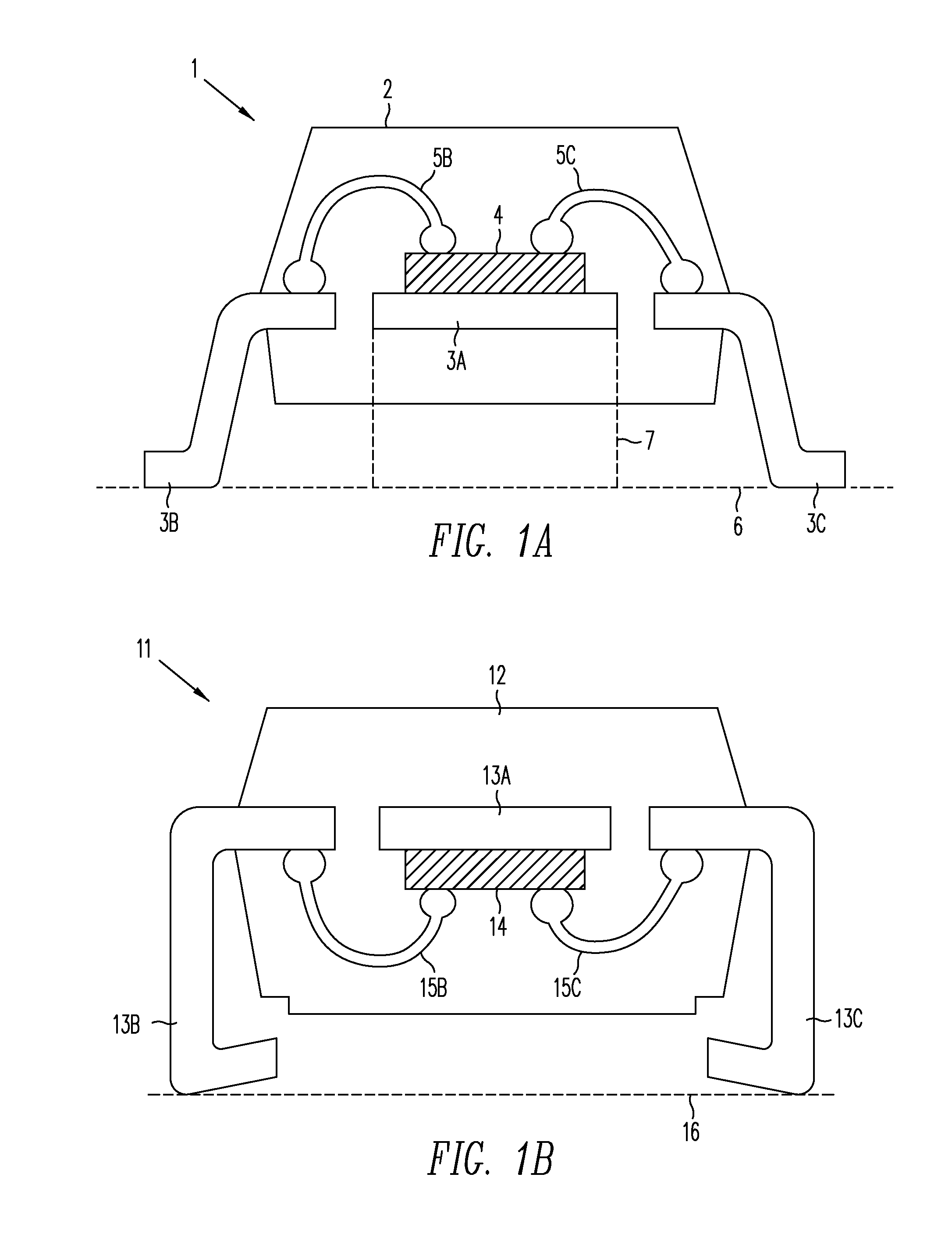
Conversely, when heat
slug 7 extends below the bottoms of leads 3B and 3C, then the leads may not solder onto the PCB whatsoever, resulting in open circuits and defective PCBs.
Worse yet, poor or “cold” solder joints may result, passing final manufacturing tests but failing during operation in the field.
Significant field failures can result in costly product recalls with the potential for customer damage claims against the manufacturer.
If any of these intervening regions are not filled with solder 30, an undesirable void will result, weakening the
mechanical strength of the solder joint, increasing the electrical resistance of the connection, and possibly compromising the reliability of the product.
Eventually, a crack will form in the solder, and the component will develop and open or intermittent
electrical connection.
Since, however, the main solder connection is “beneath” the component,
visual inspection is not possible, so that expensive x-
ray inspection equipment is required.
Such products typically command sufficiently high prices to afford the higher manufacturing cost of a multilayer PCB
assembly facility.
Some markets, however, are extremely
cost sensitive and cannot afford the high cost of multilayer PCBs or reflow PCB assembly with x-
ray inspection.
These old PCB factories are incapable of reflow solder manufacturing, lack x-
ray inspection equipment, and can accommodate only one- or at most two-sided PCBs, i.e. PCBs with only one or two conductive
layers.
Despite their performance advantages, leadless packages are intrinsically incompatible with
wave soldering and low cost PCB assembly.
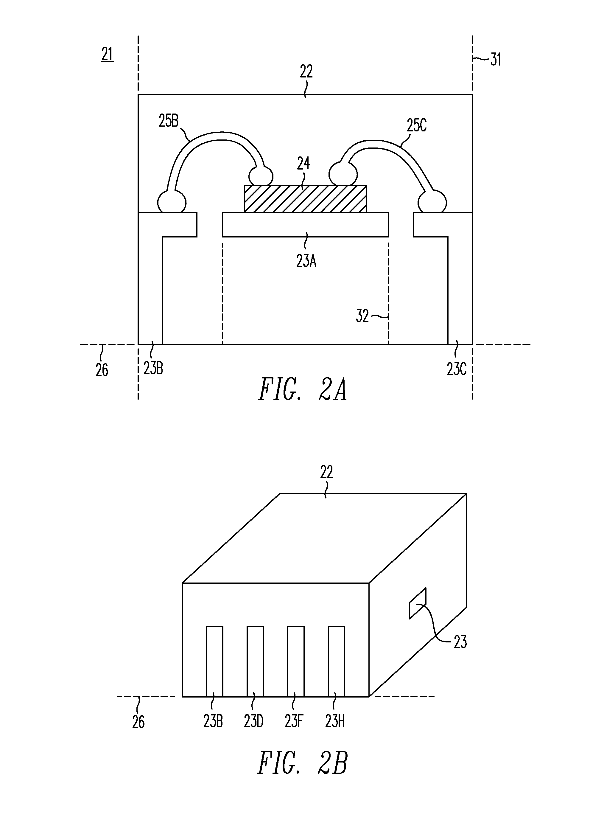
Likewise, the vertical edges of the exposed leads 23B and 23C of the leadless package 21 shown in FIG. 2A are not suitable for wave-solder assembly because the solder will not reliably wick its way onto a vertical exposed lead, in essence because it is too steeply inclined.
Also, as a
vertical edge, it is impractical to visually inspect solder coverage of the lead.
Unfortunately, the angle of the side of a leadless package is necessarily vertical because of the way in which it is manufactured. FIG. 3 illustrates a leadless package during manufacturing after
plastic molding but before singulation.
As a result, all leadless packages today lack the ability to be assembled using low cost wave solder PCB factories.
In conclusion, leaded packages such as the gull wing, JW-type, and LQFP plastic packages are compatible with low cost wave-solder PCB assembly and
visual inspection, but suffer from a high package height, problems with maintaining precise coplanarity of the leads during the bending process, poor area efficiency, and an inability to incorporate a heat
slug for improved power dissipation.
Leadless packages like the DFN and QFN offer superior coplanarity, high area efficiency, and the ability to incorporate a heat slug for improved power dissipating capability, but are incompatible with low cost PCB assembly using wave-
soldering and
visual inspection, instead requiring more expensive solder reflow PCB manufacturing with x-ray inspection.

