

Layout Structure of Heterojunction Bipolar Transistors
a bipolar transistor and layout structure technology, applied in semiconductor devices, semiconductor/solid-state device details, electrical apparatus, etc., can solve the problems of limiting the competitiveness of products, reducing the efficiency of packaging, and low uniform height of copper pillars, so as to improve heat dissipation efficiency of devices, reduce the height difference between emitter and collector copper pillars in the conventional flip-chip technology, and flexible layout design of emitter and collector copper pillars
- Summary
- Abstract
- Description
- Claims
- Application Information
AI Technical Summary
Benefits of technology
Problems solved by technology
Method used
Image

Examples
Embodiment Construction
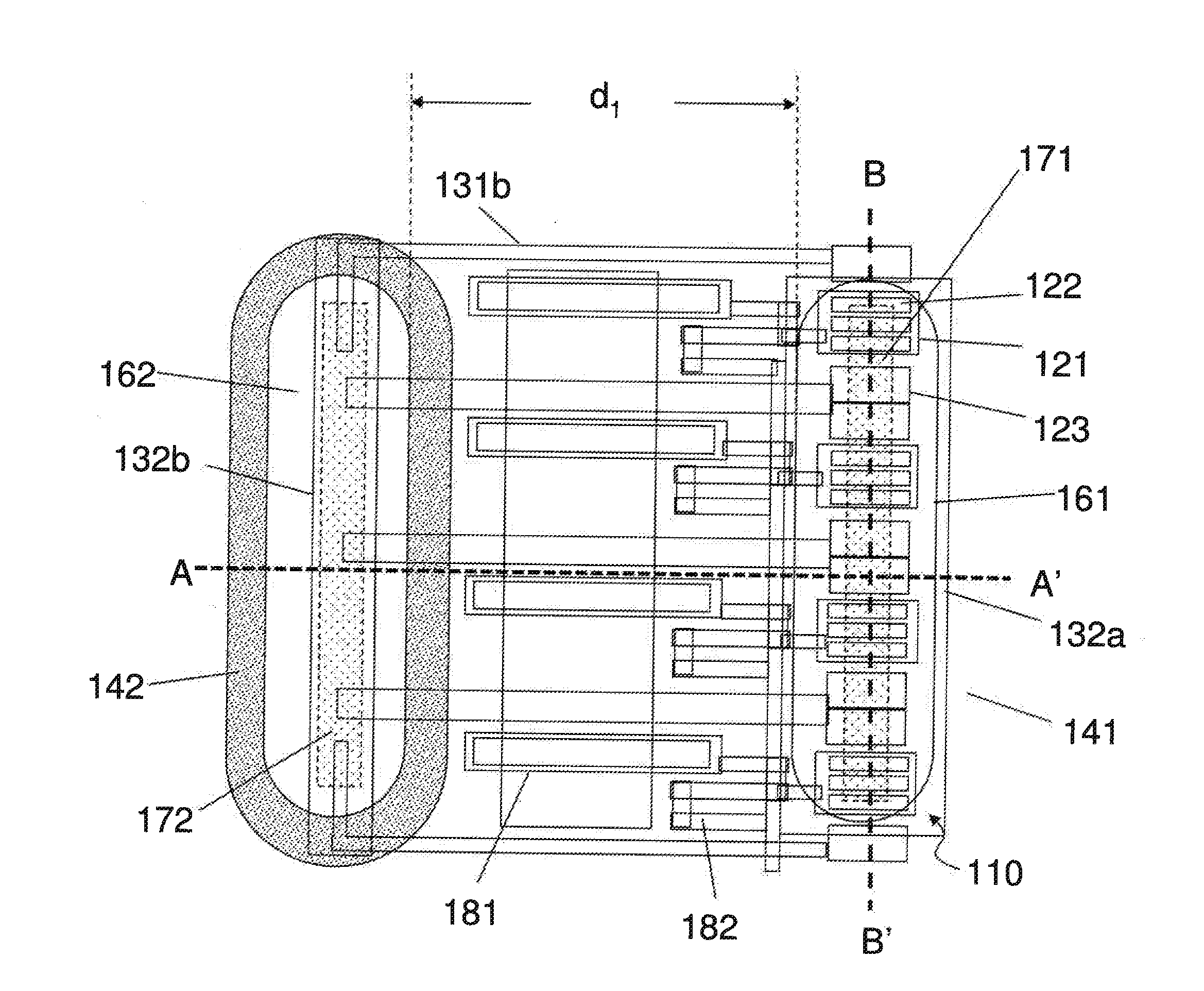
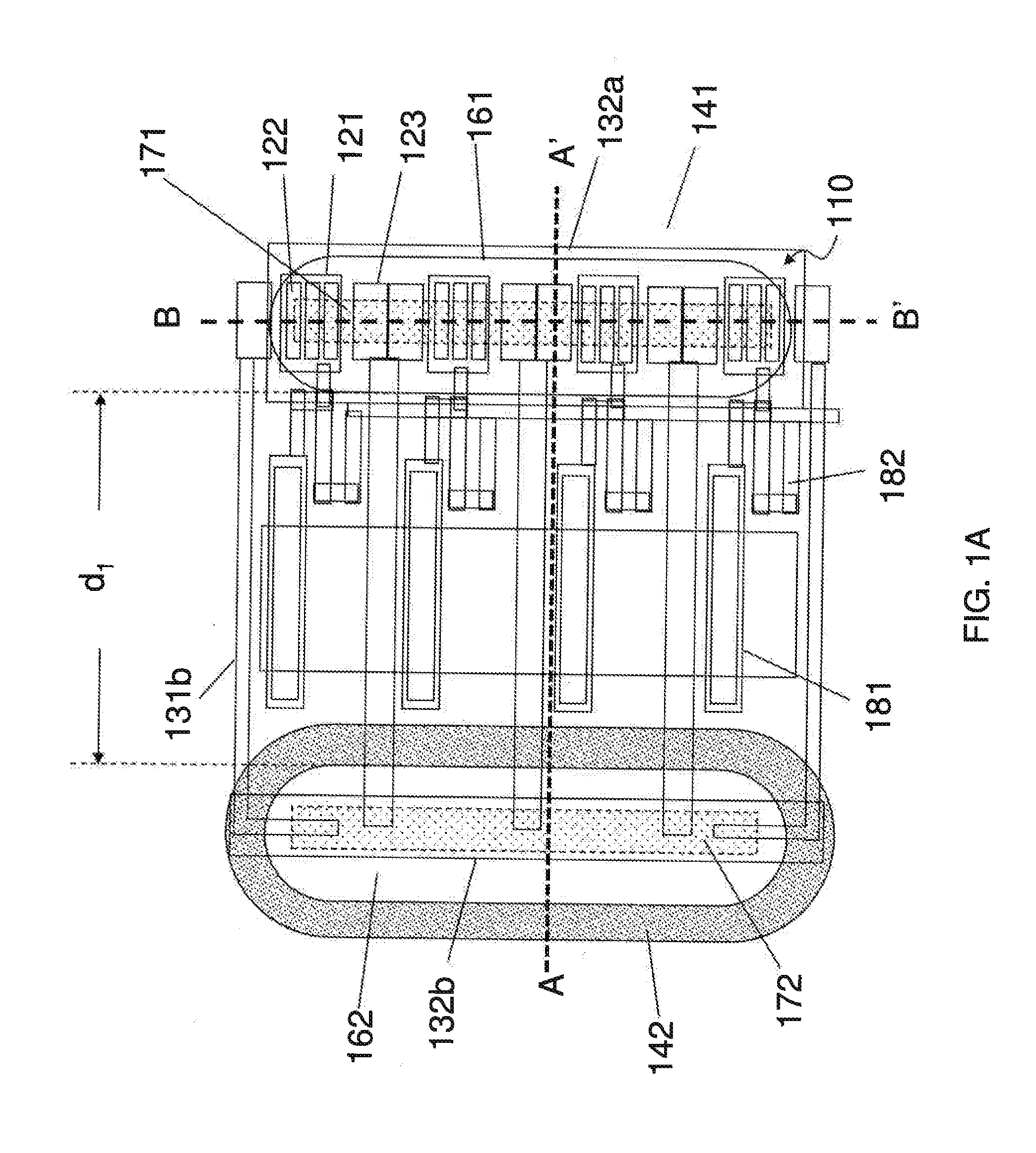
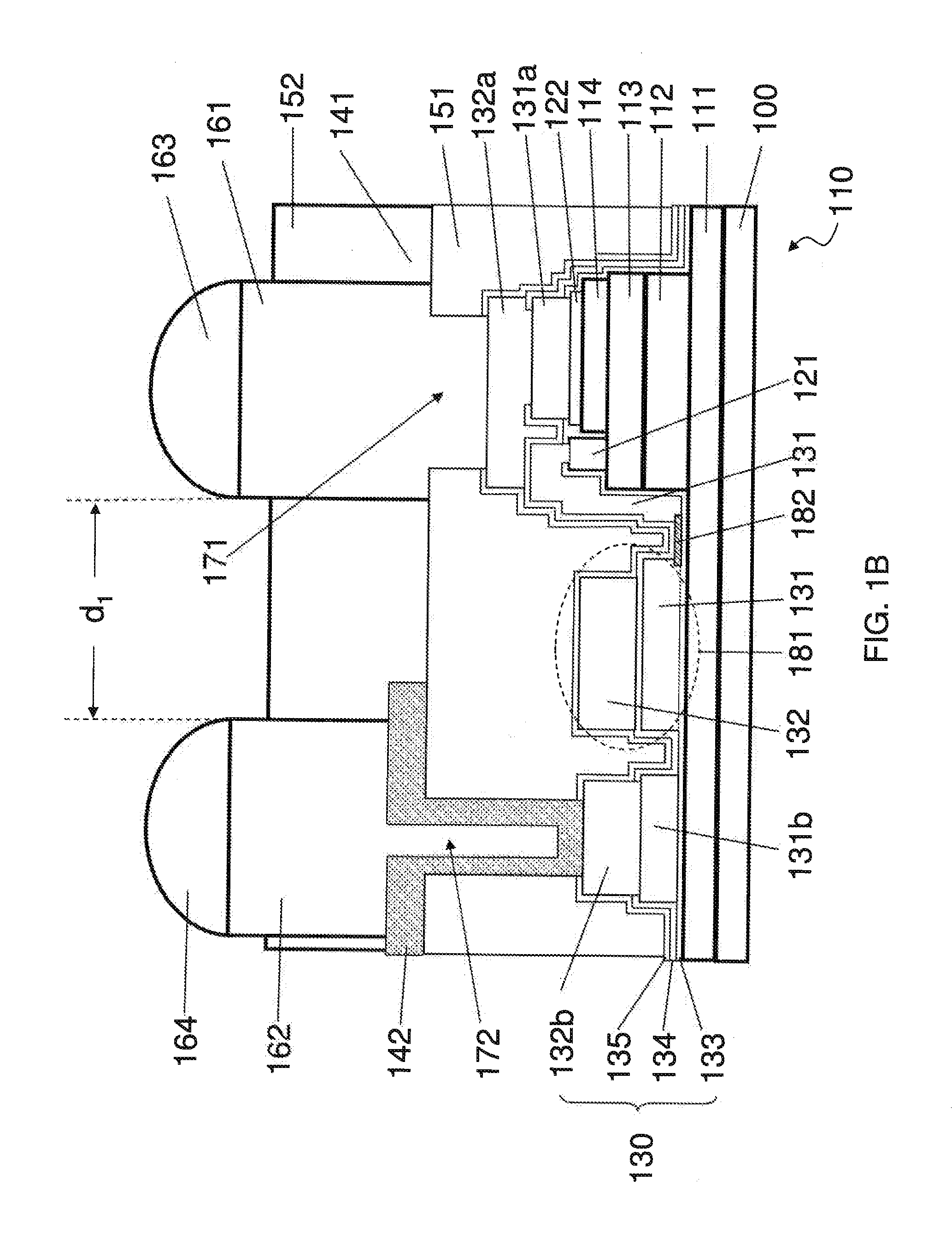
[0023]FIG. 1A-1C are schematics showing an embodiment of a layout structure of HBTs provided by the present invention, in which FIGS. 1B and 1C are the cross-sectional views along line AA′ and BB′ respectively in FIG. 1A. As shown in the figures, the layout structure of HBTs comprises one or more HBTs 110, a passive layer 130, a first dielectric layer 151, a collector redistribution layer 142, an emitter copper pillar 161, and a collector copper pillar 162. The one or more HBTs 110 are formed on a substrate 100. Each of the one or more HBTs comprises a sub-collector layer 111, a collector layer 112, a base layer 113, and an emitter layer 114. In each of the HBTs, a base electrode 121 is provided on the base layer 113, an emitter electrode 122 is provided on the base layer 114, and a collector electrode 123 is provided on the collector layer 111. The passive layer 130 is formed on the HBTs 110 and comprises an emitter pad 131a and a collector pad 132b. The emitter pad 131a is electri...
PUM
 Abstract
Description
Claims
Application Information