Flexible semiconductor devices based on flexible freestanding epitaxial elements

a technology of flexible freestanding epitaxial elements and semiconductor devices, which is applied in the direction of chemically reactive gases, crystal growth processes, chemistry apparatuses and processes, etc., can solve the problems of limited speed and cost of semiconductor device layer growth loss of the benefit of growing on the flexible epitaxial element, and damage to the addition layer of the device, etc., to reduce the processing time of growing the layer, improve the epitaxial quality, and reduce the defect density

Active Publication Date: 2014-10-30
GOLDENEYE
View PDF2 Cites 5 Cited by
  • Summary
  • Abstract
  • Description
  • Claims
  • Application Information

AI Technical Summary

Benefits of technology

[0019]Stress is a major concern in growing semiconductor devices like LEDs. Radius of curvature of the growth substrate is typically monitored in-situ to minimize the stresses during critical growth steps such as quantum well growth. Typically the goal is to increase the radius of curvature to greater than 1 km during critical growth steps. In general, the semiconductor industry is attempting to increase the radius of curvature (e.g. flatten wafers). Non-flat wafers can have non-uniform heating when heating platens are used in the growth reactor. It is inherent to epitaxial growth however that thermal mismatch will occur in any subsequent growth steps. Flexible epitaxial elements approach the problem from the opposite direction, as the flexible epitaxial element flexes, stresses can be reduced. In addition, the elemental composition of the epitaxial layers will change based on surface stresses. It has been observed with the epitaxial elements of this invention that their inherent flexibility enables higher indium compositions due to the lower surface stresses during growth of the additional semiconductor layers.

Problems solved by technology

If the thinning occurs prior to deposition of the additional layers, damage will occur to the as grown virgin epi ready surface and if the thinning occurs after the deposition of the additional layers the additional layers can be damaged and the benefit of growing on a flexible epitaxial element are lost.
The quality, accuracy, speed and cost of the semiconductor device layer growths on the epitaxial element are limited by the rate at which the epitaxial element can be heated and cooled.
This results in the need for slower growth rates which in turn increase the time it takes to grow the device.
Non-flat wafers can have non-uniform heating when heating platens are used in the growth reactor.
It is inherent to epitaxial growth however that thermal mismatch will occur in any subsequent growth steps.

Method used


Image

  • Flexible semiconductor devices based on flexible freestanding epitaxial elements
  • Flexible semiconductor devices based on flexible freestanding epitaxial elements
  • Flexible semiconductor devices based on flexible freestanding epitaxial elements

Examples


Embodiment Construction

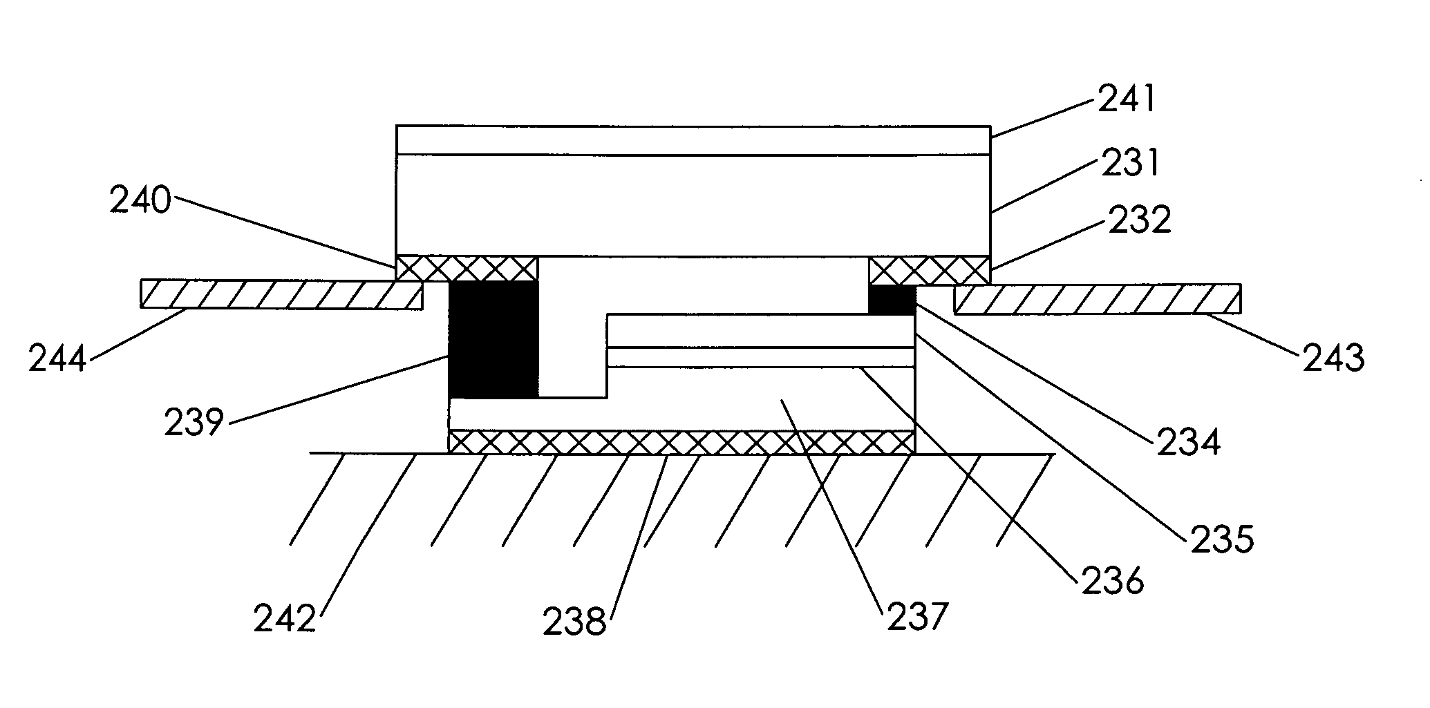
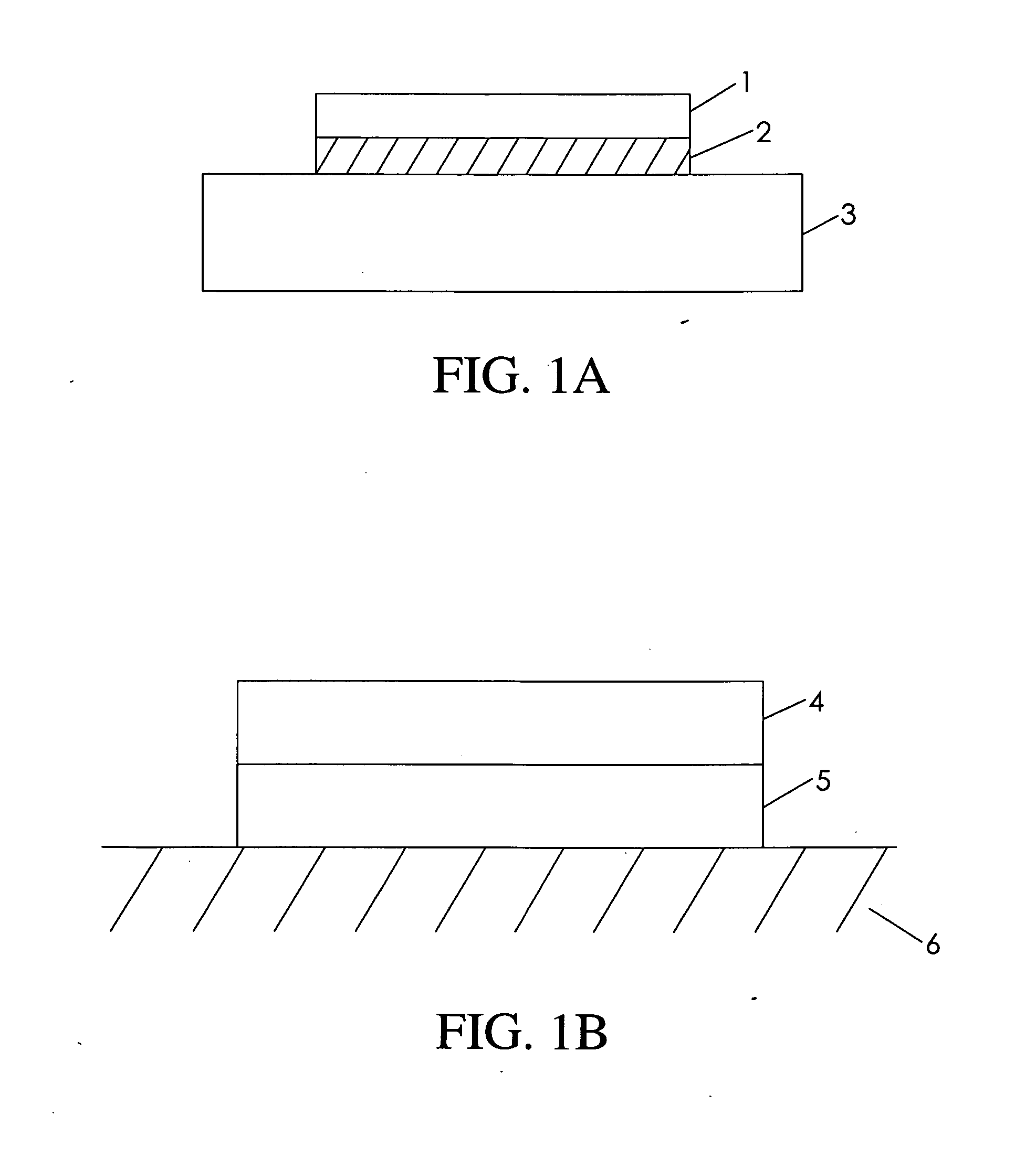
[0115]FIG. 1A depicts a typical waferbonded nitride device as seen in high powered LEDs. In this case, the flexible freestanding epitaxial element 1 typically contains a MQW structure and associated contact layers and metallizations as known in the art. The flexible freestanding epitaxial element 1 is attached via solder layer 2 to support 3, which is typically a thermally conductive material like silicon, germanium, or metal composites. The typical thickness of the flexible freestanding epitaxial element 1 is less than 3 microns and the flexible freestanding epitaxial element 1 lacks the mechanical integrity to be handled or processes without being attached to support 3. In addition, the stresses with the flexible freestanding epitaxial element 1 cause it to warp significantly if it were not attached to support 3. The thermal impedance through the solder layer 2 and support 3 determines the maximum power density of the device. Alternately FIG. 1 B depicts a flexible freestanding ep...


PUM


Abstract

Flexible semiconductor devices based on flexible freestanding epitaxial elements are disclosed. The flexible freestanding epitaxial elements provide a virgin as grown epitaxy ready surface for additional growth layers. These flexible semiconductor devices have reduced stress due to the ability to flex with a radius of curvature less than 100 meters. Low radius of curvature flexing enables higher quality epitaxial growth and enables 3D device structures. Uniformity of layer formation is maintained by direct absorption of actinic radiation by the flexible freestanding epitaxial element within a reactor. In addition, standard post processing steps like lithography are enabled by the ability of the devices and elements to be flattened using a secondary support element or vacuum. Finished flexible semiconductor devices can be flexed to a radius of curvature of less than 100 meters. Nitrides, Zinc Oxides, and their alloys are preferred materials for the flexible freestanding epitaxial elements.

Description

REFERENCE TO PRIOR APPLICATION[0001]This application is a continuation of U.S. application Ser. No. 12 / 462,295 filed Jul. 31, 2009 which claims the benefit of U.S. Provisional Patent Application Ser. No. 61 / 188,115, which was filed on Aug. 4, 2008, all commonly assigned as the present application and herein incorporated by reference.BACKGROUND OF THE INVENTION[0002]Flexible semiconductor devices offer several advantages over more conventional wafer based semiconductor devices for mobile devices, wearable devices, and lower cost devices. Flexibility is usually defined by the radius of curvature in kilometers that the flexible semiconductor device can be flexed to. In general, flexible semiconductor devices in the prior art are formed in a wafer state and then either removed from a growth substrate, thinned, or otherwise separated from a rigid element. While this allows for processing using standard semiconductor wafer based lithography or patterning equipment tool sets, a critical be...

Claims


Application Information

Patent Timeline
Patent Type & Authority Applications(United States)
IPC IPC(8): H01L29/20
CPCH01L29/2003C30B25/18H01L21/2007H01L31/03926H01L31/1836H01L31/1852H01L33/007H01L33/32H01L2224/48091H01L2924/00014Y02E10/544H01L2224/45099H01L31/0392
Inventor ZIMMERMAN, SCOTT M.BEESON, KARL W.LIVESAY, WILLIAM R.ROSS, RICHARD L.
Owner GOLDENEYE
Why Eureka
Try Eureka