Lead frame, method for manufacturing lead frame, semiconductor device, and method for manufacturing semiconductor device

a lead frame and lead frame technology, applied in the direction of semiconductor devices, solid-state devices, basic electric elements, etc., can solve the problems of increased manufacturing cost of the package, difficulty in ensuring mounting reliability, and increase in the length of the bonding wire, and achieve the effect of small thickness

Active Publication Date: 2014-10-30
DAI NIPPON PRINTING CO LTD
View PDF3 Cites 18 Cited by
  • Summary
  • Abstract
  • Description
  • Claims
  • Application Information

AI Technical Summary

Benefits of technology

[0049]According to the present invention, there is provided a lead frame for a semiconductor device, the lead frame including: a die pad on which a semiconductor element is to be mounted; and a plurality of long lead portions and a plurality of short lead portions provided on a periphery of the die pad; wherein a plurality of short lead portions are arranged so as to be adjacent to each other in a vicinity of a corner portion of a region corresponding to the semiconductor device; and wherein the plurality of short lead portions are coupled to each other through a coupling body having a rear surface formed such that the coupling body has a small thickness.
[0050]According to the present invention, a solder portion connecting an external terminal disposed at a position close to a corner portion of the die pad to an external mounting board can be prevented from being cracked due to effects of thermal expansion and contraction.

Problems solved by technology

However, the package of a QFN having a conventional ordinary structure becomes larger as the number of terminals increases, making it difficult to ensure mounting reliability.
The larger size of the package lengthens distance between internal terminals and a semiconductor chip, and therefore increases an amount of usage of bonding wires made of gold, so that the manufacturing cost of the package rises.
In addition, an increase in length of the bonding wires may cause a problem at a time of package assembly.
The small width may make the strength of the half-etched lead portions insufficient, possibly deforming the lead portions to cause displacement of external terminals.

Method used


Image

  • Lead frame, method for manufacturing lead frame, semiconductor device, and method for manufacturing semiconductor device
  • Lead frame, method for manufacturing lead frame, semiconductor device, and method for manufacturing semiconductor device
  • Lead frame, method for manufacturing lead frame, semiconductor device, and method for manufacturing semiconductor device

Examples


first embodiment

[0081]A first embodiment of the present invention will be described below with reference to FIGS. 1 to 9(e).

Structure of Lead Frame

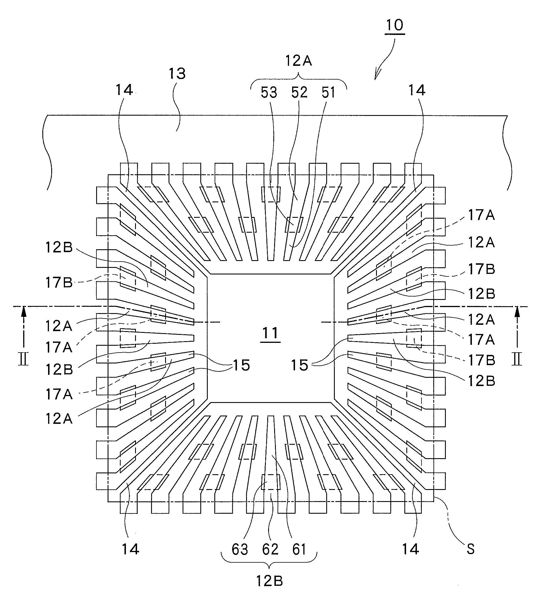
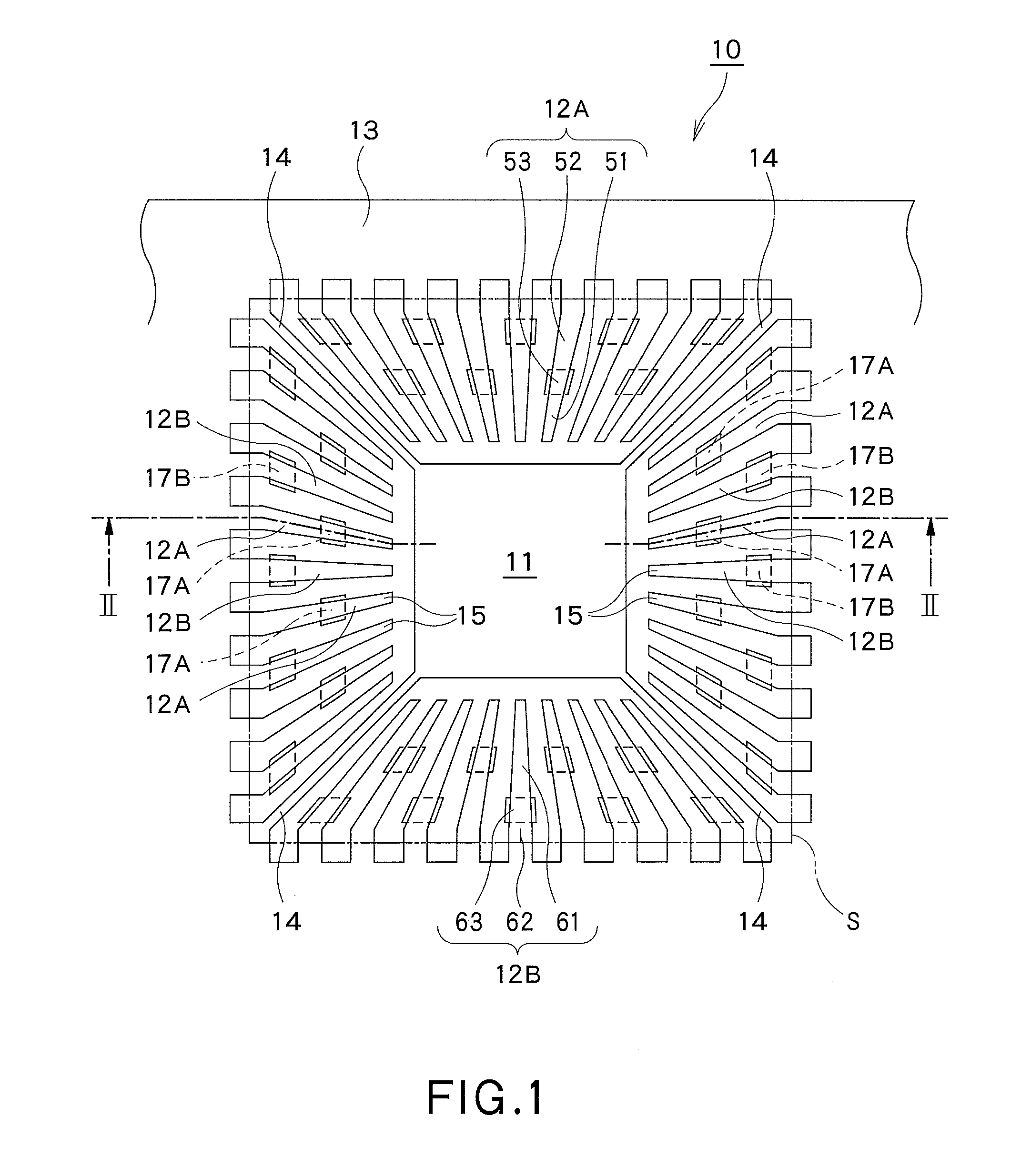
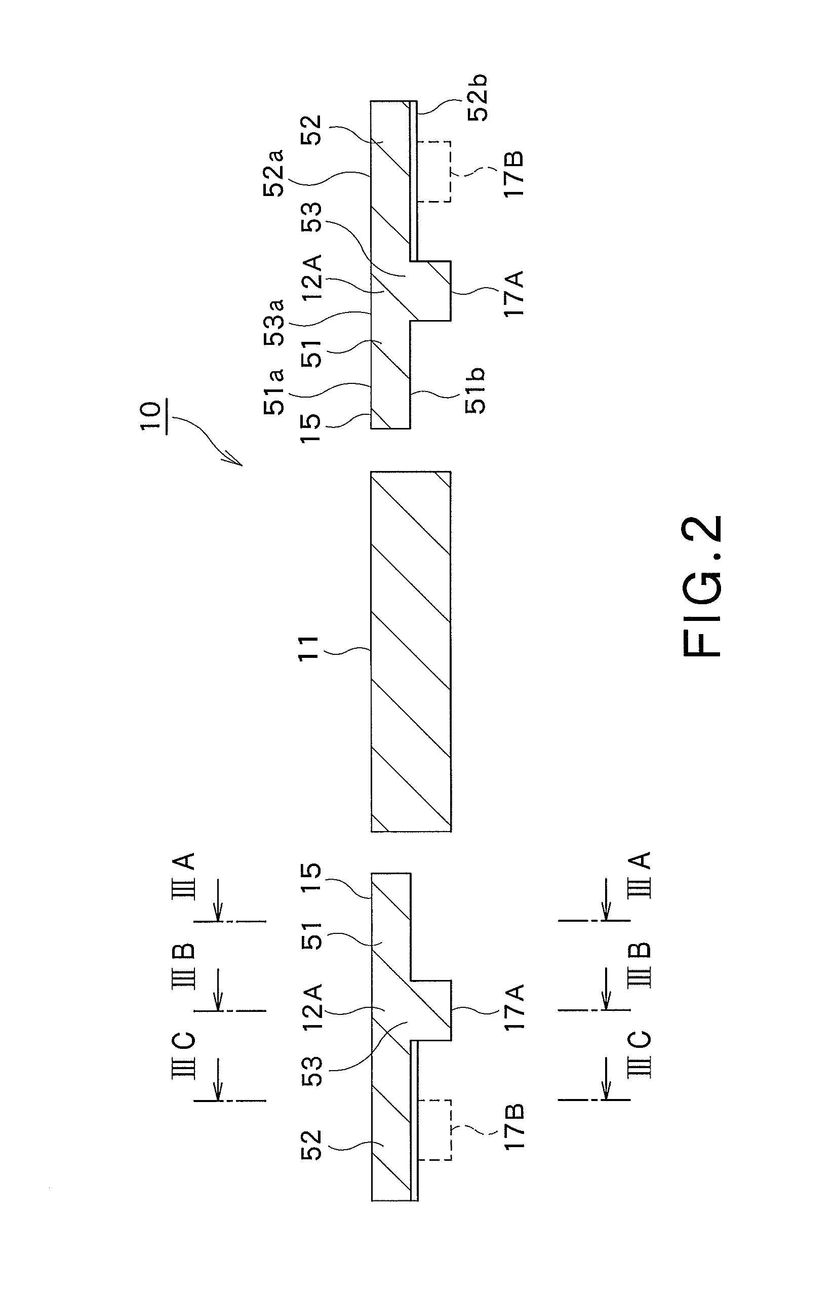
[0082]Outlines of a lead frame according to the present embodiment will first be described with reference to FIGS. 1 to 3(c). FIGS. 1 to 3(c) are diagrams showing the lead frame according to the present embodiment.

[0083]As shown in FIG. 1 and FIG. 2, the lead frame 10 includes a die pad 11 of a rectangular planar shape, on which die pad a semiconductor element 21 (to be described later) is to be mounted, and a plurality of elongate lead portions 12A and 12B provided on the periphery of the die pad 11 to connect the semiconductor element 21 to an external circuit (not shown).

[0084]An outer frame 13 supporting the die pad 11 and the lead portions 12A and 12B is provided on the periphery of the lead portions 12A and 12B. Further, suspension leads 14 are coupled to four corners of the die pad 11 that is coupled to and supported by the outer frame 13 via the ...

second embodiment

Modification of Second Embodiment

[0169]A modification of the second embodiment of the present invention will now be described with reference to FIGS. 18 to 20(b). FIGS. 18 to 20(b) are diagrams showing a modification of the second embodiment of the present invention. The modification shown in FIGS. 18 to 20(b) is different in terms of the cross-sectional shape of outside regions 52, and is substantially identical to the foregoing first embodiment and the foregoing second embodiment in terms of other structures. In FIGS. 18 to 20(b), the same parts as in the first embodiment and the second embodiment are identified by the same reference numerals, and detailed description thereof will be omitted.

[0170]As shown in FIG. 18 and FIGS. 19(a) and 19(b), in a lead frame 10A according to the present modification, an outside region 52 has a recessed portion 52f recessed upward (in a direction of a top surface) in a cross section orthogonal to the longitudinal direction of a lead portion 12A.

[0...

third embodiment

Modifications of Third Embodiment

[0231]The foregoing embodiment has been described by taking as an example a case where the lead frame 110 has the plurality of long lead portions 116A and the plurality of short lead portions 116B, the long lead portions 116A and the short lead portions 116B being arranged alternately along the periphery of each side 115a of the die pad 115 except for both end portions of each side 115a of the die pad 115. However, without being limited to this, the lead frame 110 may have a plurality of lead portions having lengths identical to each other. And a pair of lead portions adjacent to each other which lead portions are arranged in the vicinities of the end portions of each side 115a of the die pad 115 may be coupled to each other through a coupling body 128. Alternatively, the lead frame 110 may have a plurality of lead portions whose length is gradually larger from the center of each side 115a to both end portions thereof. And a pair of lead portions adj...


PUM

PropertyMeasurementUnit
thicknessaaaaaaaaaa
thicknessaaaaaaaaaa
surface temperatureaaaaaaaaaa

Abstract

A lead frame includes a die pad and a plurality of lead portions each including an internal terminal and an external terminal. The external terminals of the plurality of lead portions are arranged in an alternately staggered form such that the respective external terminals of a pair of lead portions adjacent to each other are alternatively located on an inside or an outside. A lead portion has an inside region located on the inside of a first external terminal, an outside region located on the outside of the first external terminal, and an external terminal region having the first external terminal. The inside region and the outside region are each formed thin by means of half etching. A maximum thickness of the outside region is larger than a maximum thickness of the inside region.

Description

CROSS-REFERENCE TO RELATED APPLICATIONS[0001]The present patent application claims the benefits of Japanese Patent Application No. 2013-087713, filed in Japan on Apr. 18, 2013, Japanese Patent Application No. 2013-087695, filed in Japan on Apr. 18, 2013, and Japanese Patent Application No. 2013-201321, filed in Japan on Sep. 27, 2013. The entire disclosed content of these prior applications is incorporated herein as part of the present specification by way of reference.BACKGROUND OF THE INVENTION[0002]1. Field of the Invention[0003]The present invention relates to a lead frame and a method of manufacturing the same, and a semiconductor device and a method of manufacturing the same.[0004]2. Description of the Related Art[0005]There has recently been a demand for reductions in size and thickness of a semiconductor device mounted on a board. In order to meet such a demand, various semiconductor devices of a so-called QFN (Quad Flat Non-lead) type have conventionally been proposed which...

Claims


Application Information

Patent Timeline
Patent Type & Authority Applications(United States)
IPC IPC(8): H01L23/495H01L21/48
CPCH01L21/4828H01L23/49524H01L2224/83005H01L21/568H01L24/97H01L2224/32245H01L2224/48247H01L2224/73265H01L2224/92247H01L2224/97H01L2224/85005H01L23/3107H01L23/49541H01L23/49548H01L23/49582H01L2924/1301H01L24/73H01L2924/181H01L2224/05554H01L2924/00014H01L24/45H01L2224/45144H01L24/48H01L24/49H01L2224/49171Y10T29/49121H01L2224/49433H01L2924/18301H01L2924/00012H01L2224/83H01L2224/85H01L2924/00H01L2224/45015H01L2924/207H01L21/56H01L23/49503H01L24/83H01L24/85H01L24/92H01L2224/48245H01L23/3142H01L23/4951H01L23/49544
Inventor SHIBASAKI, SATOSHITOMITA, KOJIYAZAKI, MASAKIMIYANO, KAZUYUKIKURAHASHI, ATSUSHIUCHIUMI, KAZUHITOMASUDA, MASACHIKA
Owner DAI NIPPON PRINTING CO LTD
Why Eureka
Try Eureka