Through silicon via repair circuit of semiconductor device

a technology of through silicon and repair circuit, which is applied in the direction of semiconductor/solid-state device testing/measurement, semiconductor/solid-state device details, pulse techniques, etc., can solve the problems of tsv connection failure among the chips, short circuit between the tsv and the substrate, and increase the ic usage area and severe delay time and power consumption of signals

Active Publication Date: 2014-11-20
IND TECH RES INST
View PDF6 Cites 9 Cited by
  • Summary
  • Abstract
  • Description
  • Claims
  • Application Information

AI Technical Summary

Benefits of technology

[0009]An embodiment of the disclosure provides a through silicon repair circuit of a semiconductor device, comprising: a first chip and a second chip, one of which stacks on the other; at least two data path circuits, configured in the first chip, each of which is coupled to a corresponding one of the at least two through silicon vias, wherein each of the at least two data path circuits comprises: an input driving circuit, converting a signal input from a first signal input terminal based on a power voltage and a ground voltage and transmitting the signal to a first end of the corresponding one of the at least two through silicon vias; a through silicon via detection circuit, coupled to the first signal input terminal and the first end of the corresponding one of the at least two through silicon vias, detecting a through silicon via status of the corresponding one of the at least two through silicon vias; a memory device, receiving and keeping the through silicon via status from the through silicon via detection circuit, wherein a control terminal of the memory device is coupled to a second signal input terminal; a protection circuit, coupled to the memory device and the first end of the corresponding one of the at least two through silicon vias, determining whether or not to pull the first end of the corresponding one of the at least two through silicon vias to the ground voltage based on the through silicon via status kept by the memory device; and a power control circuit, coupled to an between the power voltage and the input driving circuit and coupled to the memory device, providing the power voltage to the input driving circuit; and an output logic circuit, configured in the second chip, generating an output signal according to signals from at least two input terminals of the output logic circuit, wherein the at least two input terminals of the output logic circuit are coupled to second ends of the at least two through silicon vias, respectively.

Problems solved by technology

As the semiconductor process technologies have developed, areas of integrated circuits (ICs) have been reduced and the number of transistors in a single IC has been increased, thereby leading to an increase in IC usage area and severe delay time and power consumption of signals.
Since layers of integrated circuits have to be stacked precisely when chips are stacked, a small stacking offset could result in TSV connection failure among the chips.
Nevertheless, in the TSV manufacturing process, a sidewall insulation layer (for example, SiO2) is easily to be damaged or intruded by external impurity when being manufactured, resulting in a short circuit between the TSV and the substrate.
Moreover, during the stack package process, an open defect may occur when TSVs in layers are being connected to each other.
However, in this case, a leakage current will flow to the substrate via the defective TSV, thereby causing drift and instability of the global substrate voltage level and signal transmission failure.
In view of this, how to self-detect defects of TSVs and repair transmitting signals is an important issue in 3-D ICs.

Method used


Image

  • Through silicon via repair circuit of semiconductor device
  • Through silicon via repair circuit of semiconductor device
  • Through silicon via repair circuit of semiconductor device

Examples


Embodiment Construction

[0021]It is understood that the following disclosure provides many different embodiments, or examples, for implementing different features of the application. Specific examples of components and arrangements are described below to simplify the present disclosure. These are, of course, merely examples and are not intended to be limiting. In addition, the present disclosure may repeat reference numerals and / or letters in the various examples. This repetition is for the purpose of simplicity and clarity and does not in itself dictate a relationship between the various embodiments and / or configurations discussed. Moreover, the formation of a feature on, connected to, and / or coupled to another feature in the present disclosure that follows may include embodiments in which the features are formed in direct contact, and may also include embodiments in which additional features may be formed interposing the features, such that the features may not be in direct contact.

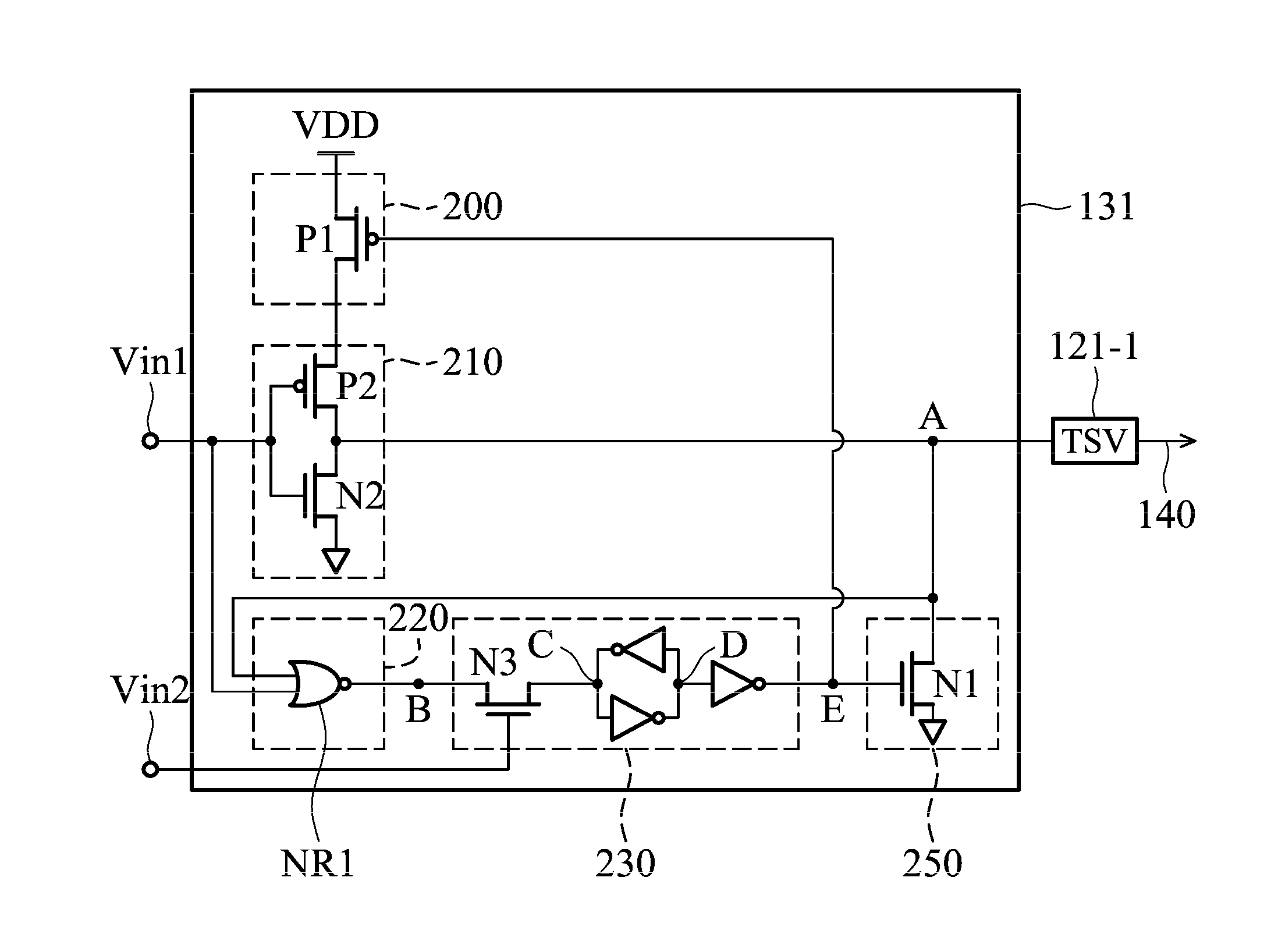
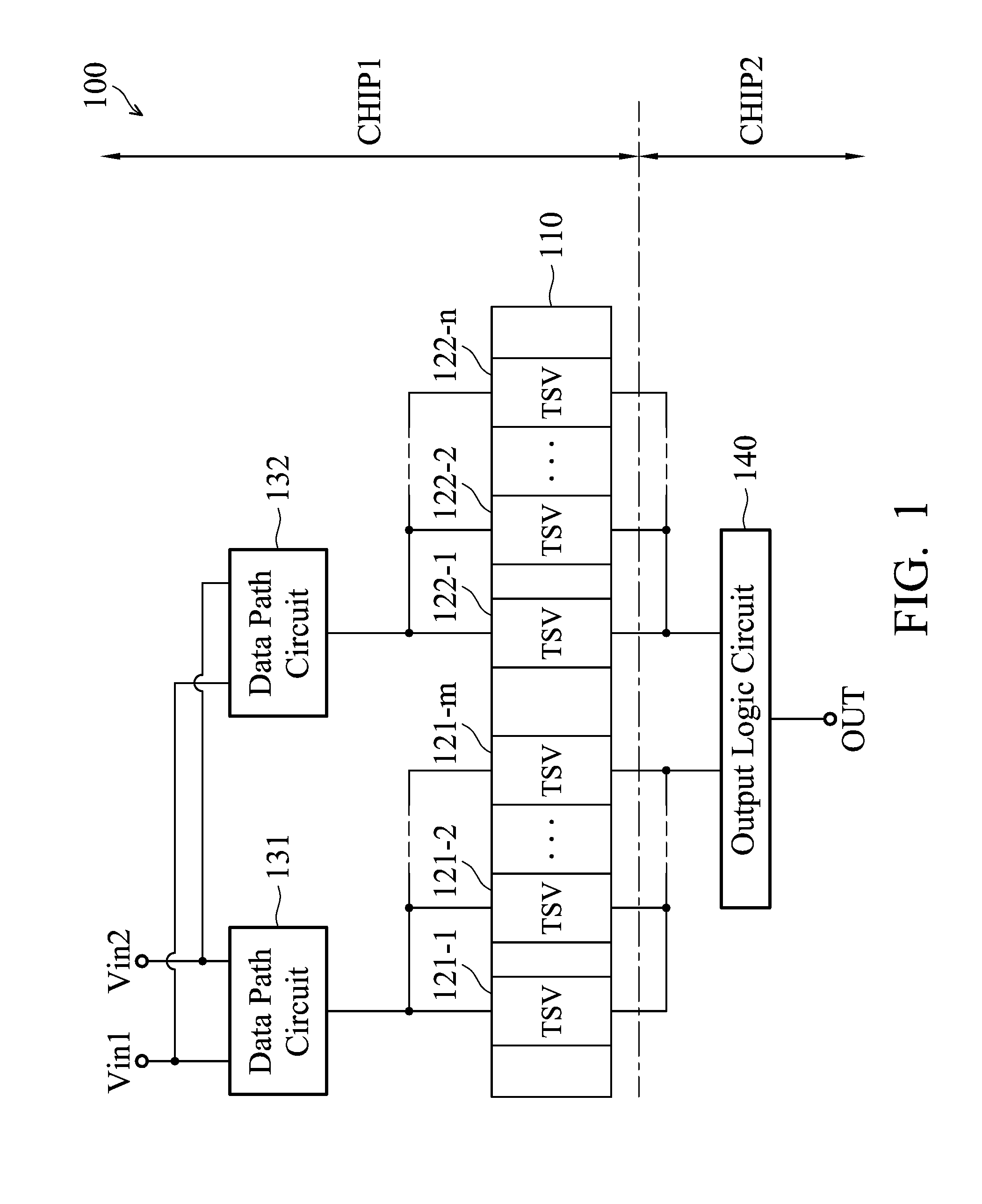
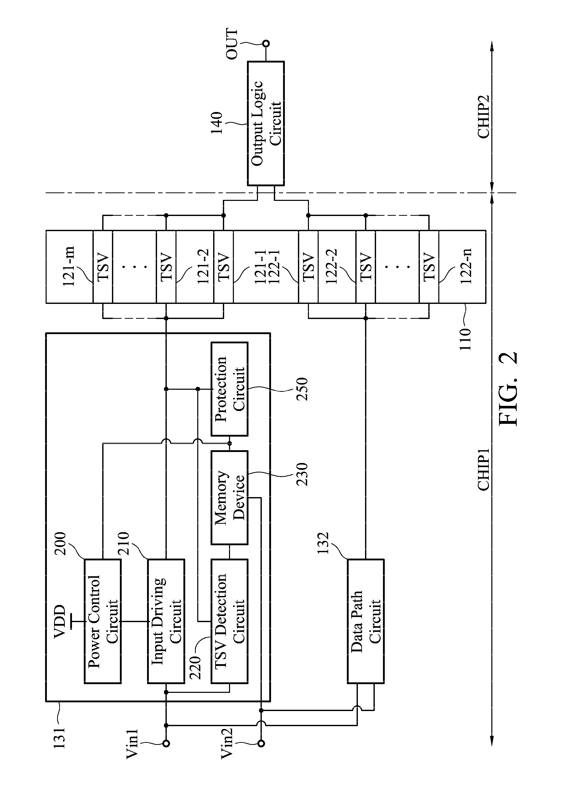
[0022]FIG. 1 is a bloc...


PUM


Abstract

TSV repair circuit of a semiconductor device includes a first chip, a second chip, at least two TSV, at least two data path circuits and an output logic circuit. Each data path circuit comprises an input driving circuit, a TSV detection circuit, a memory device, a protection circuit and a power control circuit. The TSV detection circuit detects a TSV status, the memory device keeps the TSV status, the protection circuit determines whether to pull a first end of the TSV to a ground voltage according to the TSV status, and the power control circuit prevents a leakage current of a power voltage from flowing through a substrate.

Description

CROSS REFERENCE TO RELATED APPLICATIONS[0001]This application is a Continuation-In-Part of pending U.S. patent application Ser. No. 13 / 867,122, filed on Apr. 21, 2013 and entitled “Through silicon via repair circuit of semiconductor apparatus”, which claims priority of Taiwan Patent Application No. 101144576, filed on Nov. 28, 2012, the entirety of which is incorporated by reference herein.[0002]This application claims priority of Taiwan Patent Application No. 102142945, filed on Nov. 26, 2013, the entirety of which is incorporated by reference herein.BACKGROUND[0003]1. Technical Field[0004]The disclosure relates to a through silicon via (TSV) repair circuit of a semiconductor device applied to chip stacking technologies.[0005]2. Description of the Related Art[0006]As the semiconductor process technologies have developed, areas of integrated circuits (ICs) have been reduced and the number of transistors in a single IC has been increased, thereby leading to an increase in IC usage ar...

Claims


Application Information

Patent Timeline
Patent Type & Authority Applications(United States)
IPC IPC(8): H03K19/003G01R31/28H03K19/00
CPCH03K19/003G01R31/28H03K19/0008H01L22/22H01L23/481H01L25/0657H01L2225/06544H01L2924/0002H01L2924/00H01L2225/06541
Inventor TSENG, PEI-LINGSU, KENG-LILIN, CHIH-SHENGSHEU, SHYH-SHYUAN
Owner IND TECH RES INST
Why Eureka
Try Eureka