Sample supporting member for observing scanning electron microscopic image and method for observing scanning electron microscopic image

a supporting member technology, applied in the field of scanning electron microscopic image observation techniques, can solve the problems of difficult to acquire high contrast images, and achieve the effects of high contrast images, significant gradients formed between them, and high resolution

Active Publication Date: 2014-11-27
NAT INST OF ADVANCED IND SCI & TECH
View PDF4 Cites 7 Cited by
  • Summary
  • Abstract
  • Description
  • Claims
  • Application Information

AI Technical Summary

Benefits of technology

[0029]The sample supporting member used for observing a scanning electron microscopic image according to the present invention includes the laminate of the insulative thin film and the conductive thin film; the side of the insulative thin film is an electron beam incident surface, and the side of the conductive thin film is a sample adhesion surface.
[0030]Since there are almost no free electrons in the insulative thin film on which an electron beam is incident, a negative potential is caused according to the amount of injected electrons. Accordingly, a potential difference occurs against the sample adhering side of the conductive thin film. Each of the films is a thin film. Accordingly, the potential gradient formed therebetween is significantly large. Secondary electrons occurring in the insulative thin film are released to the conductive thin film owing to the tunnel effects due to the large potential gradient, and pass through the observation sample.
[0031]Accordingly, the spatial distribution of the transmission electrons (tunnel electrons) is recorded, which allows the inner structure of the observation sample to be observed

Problems solved by technology

Unfortunately, there are problems in that such a biological sample is susceptible to dama

Method used


Image

  • Sample supporting member for observing scanning electron microscopic image and method for observing scanning electron microscopic image
  • Sample supporting member for observing scanning electron microscopic image and method for observing scanning electron microscopic image
  • Sample supporting member for observing scanning electron microscopic image and method for observing scanning electron microscopic image

Examples


Embodiment Construction

[0046]Hereinafter, referring to the drawings, a sample supporting member and a sample holder and a method for observing a scanning electron microscopic image according to the present invention are described.

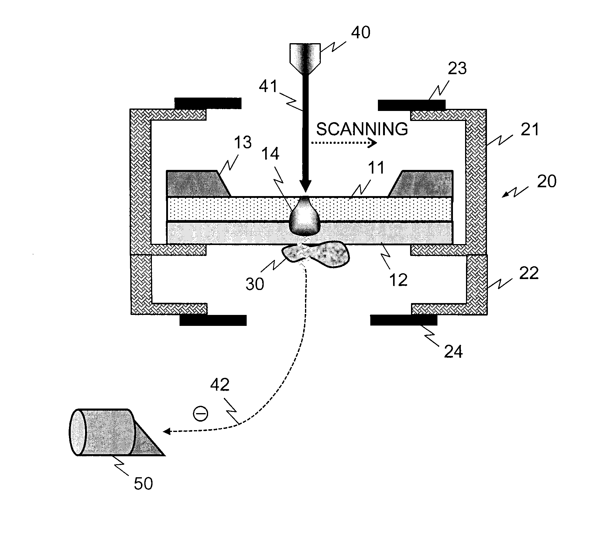
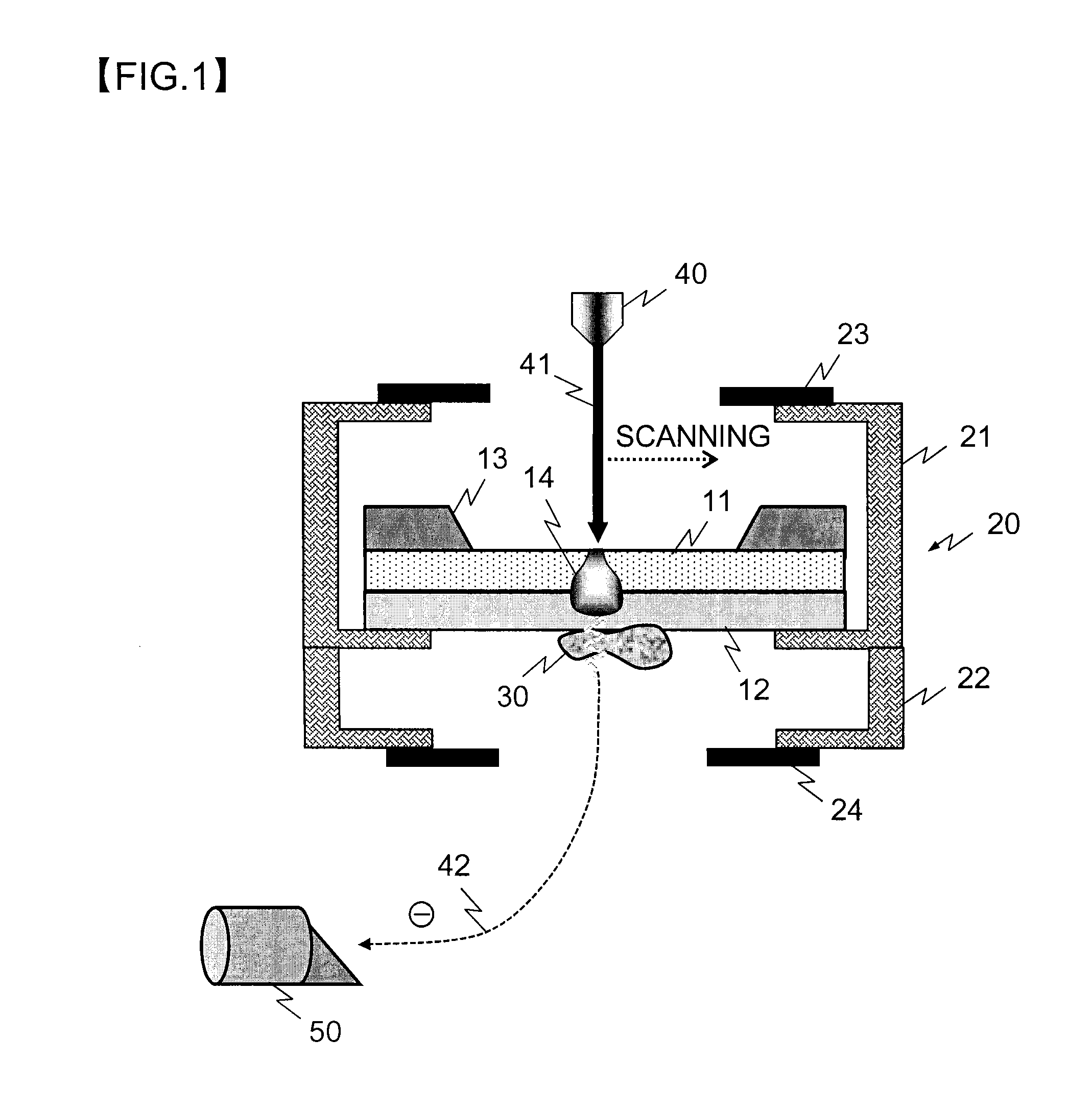
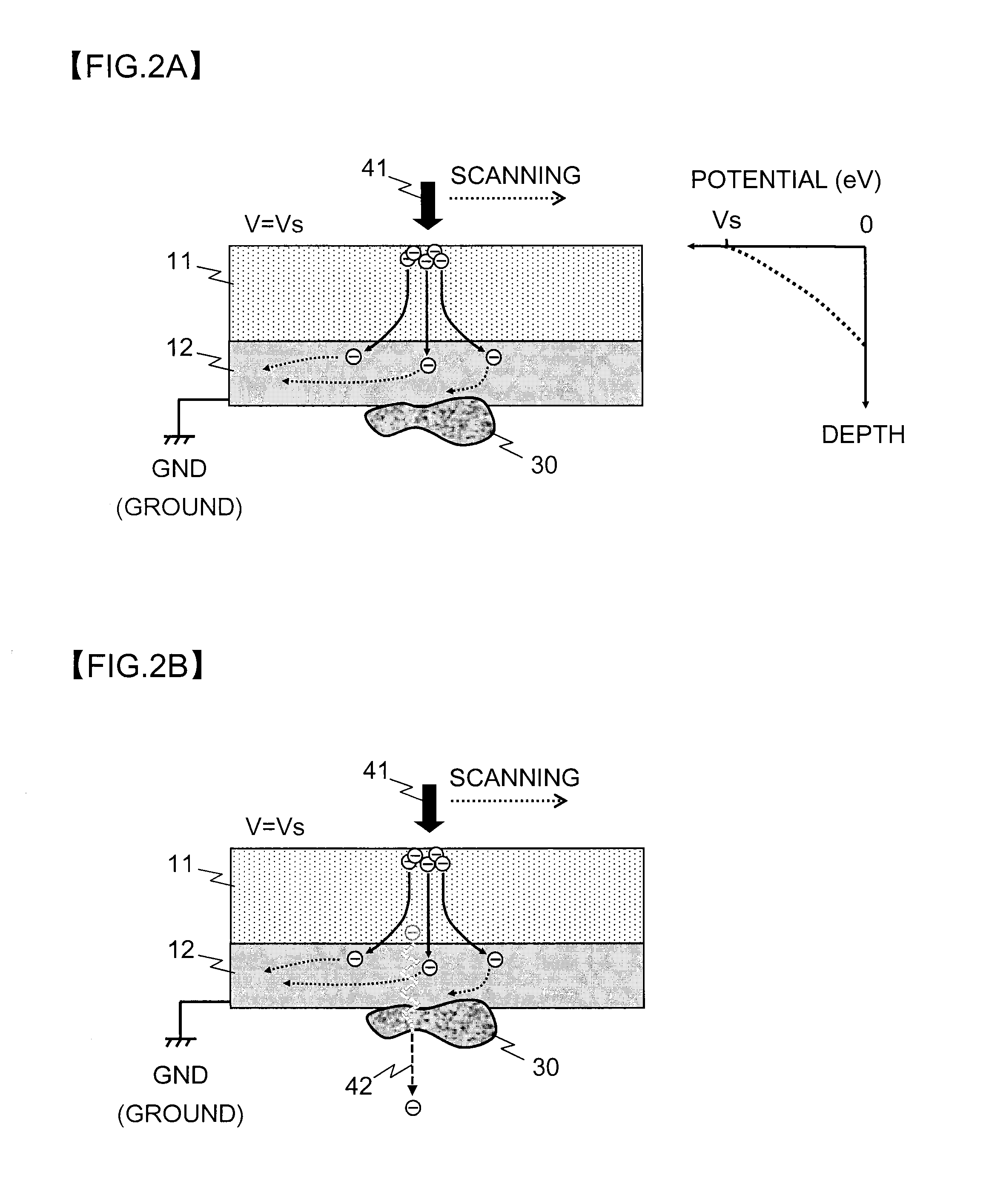
[0047]FIG. 1 is a block diagram for illustrating an overview of configurational examples of a sample supporting member and a sample holder according to the present invention. The sample supporting member is a laminate of an insulative thin film 11 and a conductive thin film 12. An electron beam 41 emitted from an electron gun 40 is incident on the insulative thin film. The undersurface of the conductive thin film 12 is a sample adhesion surface, where a sample 30 to be an observation target is held by adsorption or the like. What is indicated by sign 13 is a frame for securing a mechanical strength of the sample supporting member. The electron beam 41 scans the electron beam incident surface of the insulative thin film 11, and acquires a two-dimensional SEM image through an inten...


PUM


Abstract

When injection of electrons into a sample supporting member causes a potential gradient between an insulative thin film and a conductive thin film at a site of electron beam injection, the potential barrier of the surface of the insulative thin film becomes thin, and an electron emission phenomenon is caused by tunnel effects. Secondary electrons caused in the insulative thin film tunnel to the conductive thin film along the potential gradient. The secondary electrons, having tunneled, reach a sample while diffusing in the conductive thin film. In the case where the sample is a sample with a high electron transmittance, such as a biological sample, the secondary electrons also tunnel through the interior of the sample. The secondary electrons are detected to acquire an SEM image in which the inner structure of the sample is reflected.

Description

TECHNICAL FIELD[0001]The present invention relates to a technique for observing a scanning electron microscopic image and, in particular, to a technique suitable for observing, at high resolution, an electron microscopic image of an organic material sample and a biological sample that are susceptible to damage due to electron beam irradiation.BACKGROUND ART[0002]A scanning electron microscope (SEM) is an apparatus that has been widely used not only for morphological observation on an inorganic material sample or an organic material sample but also for observation on a biological sample, and is suitable for observing microorganisms, such as bacteria and viruses, which cannot be observed by the unaided eye.[0003]Unfortunately, there are problems in that such a biological sample is susceptible to damage due to electron beam irradiation and it is difficult to acquire a high contrast image. For SEM observation on a biological sample, typically, a sample as an observation target is pretre...

Claims


Application Information

Patent Timeline
IPC IPC(8): H01J37/20H01J37/28
CPCH01J37/20H01J2237/2813H01J37/28G21K5/08H01J2237/2003H01J2237/2004
Inventor OGURA, TOSHIHIKO
Owner NAT INST OF ADVANCED IND SCI & TECH
Why Eureka
Try Eureka