Structure and method for packaging organic photoelectric device

a photoelectric device and organic technology, applied in thermoelectric devices, basic electric elements, final product manufacturing, etc., can solve the problems of poor moisture blocking ability of organic flexible substrates, the moisture permeation of organic semiconductor materials and the moisture permeation resistance of flexible devices is still a serious problem to be overcom

Inactive Publication Date: 2014-11-27
WISTRON CORP
View PDF4 Cites 0 Cited by
  • Summary
  • Abstract
  • Description
  • Claims
  • Application Information

AI Technical Summary

Benefits of technology

[0009]According to another embodiment of the present disclosure, a structure for packaging an organic photoelectric device is disclosed. The structure includes an inorganic substrate, an organic layer, an organic photoelectric device, and a permeation barrier layer. The organic layer is disposed on the inorganic substrate. The organic photoelectric device is disposed on the organic layer

Problems solved by technology

However, the moisture permeation of the organic semiconductor materials is still a serious problem to be overcome.
However, the flexible devices become more vulnerable to be deteriorated by moisture due to the organic photoelectric devices.
Due to the poor moisture blocking ability of the organic flexible substrate, an inorganic material layer is required to be coated thereon to isolate the moisture.
However, even if the

Method used


Image

  • Structure and method for packaging organic photoelectric device
  • Structure and method for packaging organic photoelectric device
  • Structure and method for packaging organic photoelectric device

Examples


first embodiment

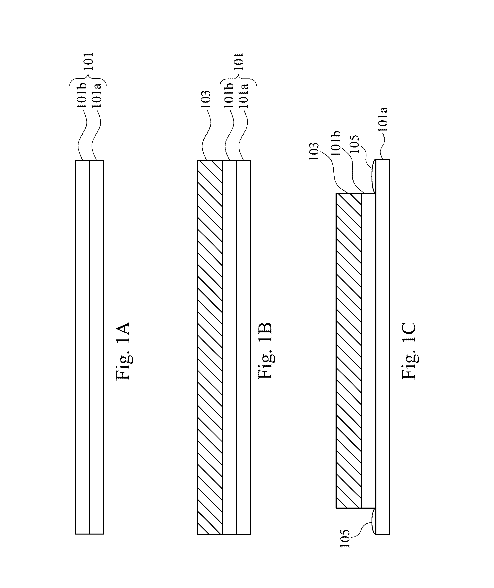
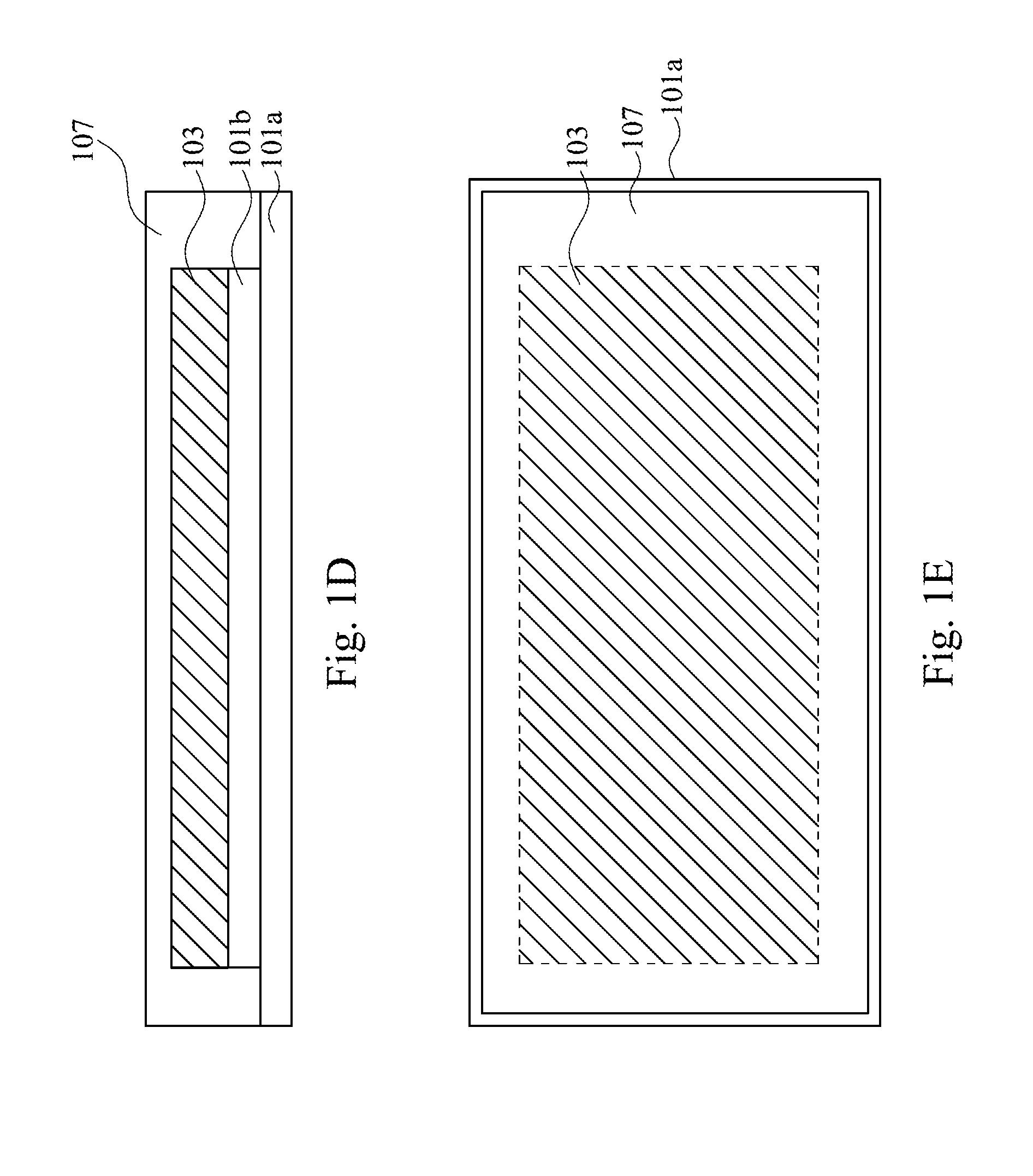
[0026]FIG. 1E is a top view of the structure for packaging the organic photoelectric device during the manufacturing process according to the present disclosure. As shown in the top view, a cross-sectional area of the permeation barrier layer 107 is greater than the cross-sectional area of the organic photoelectric device 103 but is substantially equal to the cross-sectional area of the inorganic substrate 101a. Thus, the entire organic photoelectric device 103 is covered with the permeation barrier layer 107 and is prevented from being damaged by the moisture.

second embodiment

[0027]FIG. 2A to FIG. 2C are diagrams of a structure for packaging the organic photoelectric device during a Roll-to-Roll manufacture process according to the present disclosure. A Roll-to-roll process is highly efficient and can perform the production continuously, it is generally applied on flexible material, such as films, plastics, or stainless steel sheets. In addition, metal substrates which are thin enough (thickness of about 203 is unwound from the roller 201, organic photoelectric devices 205 are set on the substrate 203. In the Roll-to-Roll process, the manufacturing of the organic photoelectric devices 205 depends on the materials and kinds of processes. The Roll-to-Roll process is substantially applied on the patterning lithography steps such as the coating step, photo-resister disposing step, exposure step, etching step, and the photo-resister removing step, to produce the organic photoelectric devices.

[0028]Then, a laser ablation process is performed for patterning in ...

third embodiment

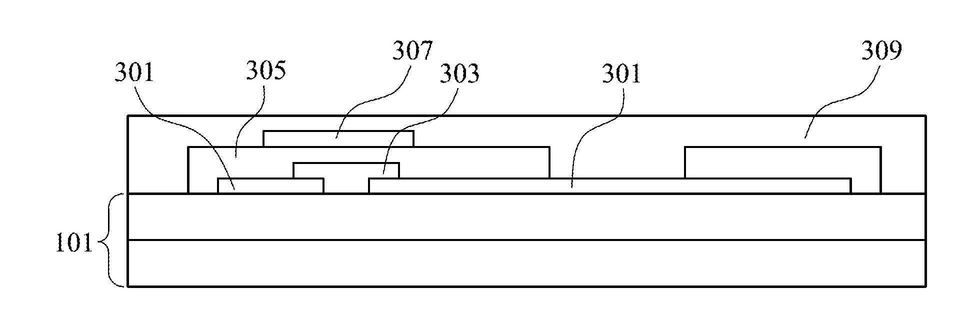
[0031]FIG. 3A to FIG. 3E are cross-sectional structure diagrams of an organic photoelectric device during a manufacturing process according to the present disclosure. In the manufacturing of the organic photoelectric devices, a metal layer 301, a semiconductor layer 303, a dielectric layer 305, a gate layer 307, and an intermediate layer 309 are sequentially stacked on a hybrid substrate 101. In other words, the semiconductor layer 303 is disposed on the metal layer 301; the dielectric layer 305 is disposed on the semiconductor layer 303; the gate layer 307 is disposed on the dielectric layer 305; and the intermediate layer 309 is disposed on the gate layer 307. Particularly, the intermediate layer 309 covers each layer of the organic photoelectric device and contacts with the hybrid substrate 101.

[0032]FIG. 4A to FIG. 4C are current-voltage curve diagram of the organic photoelectric devices. FIG. 4A presents the current-voltage curve of the organic photoelectric device without the ...


PUM


Abstract

A method for packaging an organic photoelectric device is disclosed. In the method, an inorganic substrate is provided, an organic layer is coated or pasted on the inorganic substrate to form a hybrid substrate. An organic photoelectric device is formed on the hybrid substrate, and the organic layer and the organic photoelectric device are patterned to define a package region. A permeation barrier layer is disposed on the package region to cover the organic photoelectric device.

Description

RELATED APPLICATIONS[0001]This application claims priority to Taiwanese Application Serial Number 102118664, filed May 27, 2013, which is herein incorporated by reference.BACKGROUND[0002]1. Field of Disclosure[0003]The present disclosure relates to a package structure. More particularly, the present disclosure relates to the package structure of an organic photoelectric device.[0004]2. Description of Related Art[0005]Organic photoelectric devices are mostly composed of organic semiconductors. The organic photoelectric devices have been applied on various products such as organic light-emitting diodes, organic thin film transistors, and organic solar cells. In that organic semiconductor materials are very sensitive to moistures, oxygen and ultraviolet light, stacking or shielding of certain materials may prevent the organic semiconductor materials from damages caused by oxygen and UV rays. However, the moisture permeation of the organic semiconductor materials is still a serious prob...

Claims


Application Information

Patent Timeline
IPC IPC(8): H01L51/44
CPCH01L51/448Y02E10/549H10K71/00H10K30/88Y02P70/50
Inventor KAO, CHI-JENHU, TARNG-SHIANGWANG, YI-KAICHIANG, KO-YU
Owner WISTRON CORP
Why Eureka
Try Eureka