
Nor-based bcam/tcam cell and array with NAND scalability

Active Publication Date: 2014-11-27
APLUS FLASH TECH
View PDF6 Cites 26 Cited by
  • Summary
  • Abstract
  • Description
  • Claims
  • Application Information

AI Technical Summary

Benefits of technology

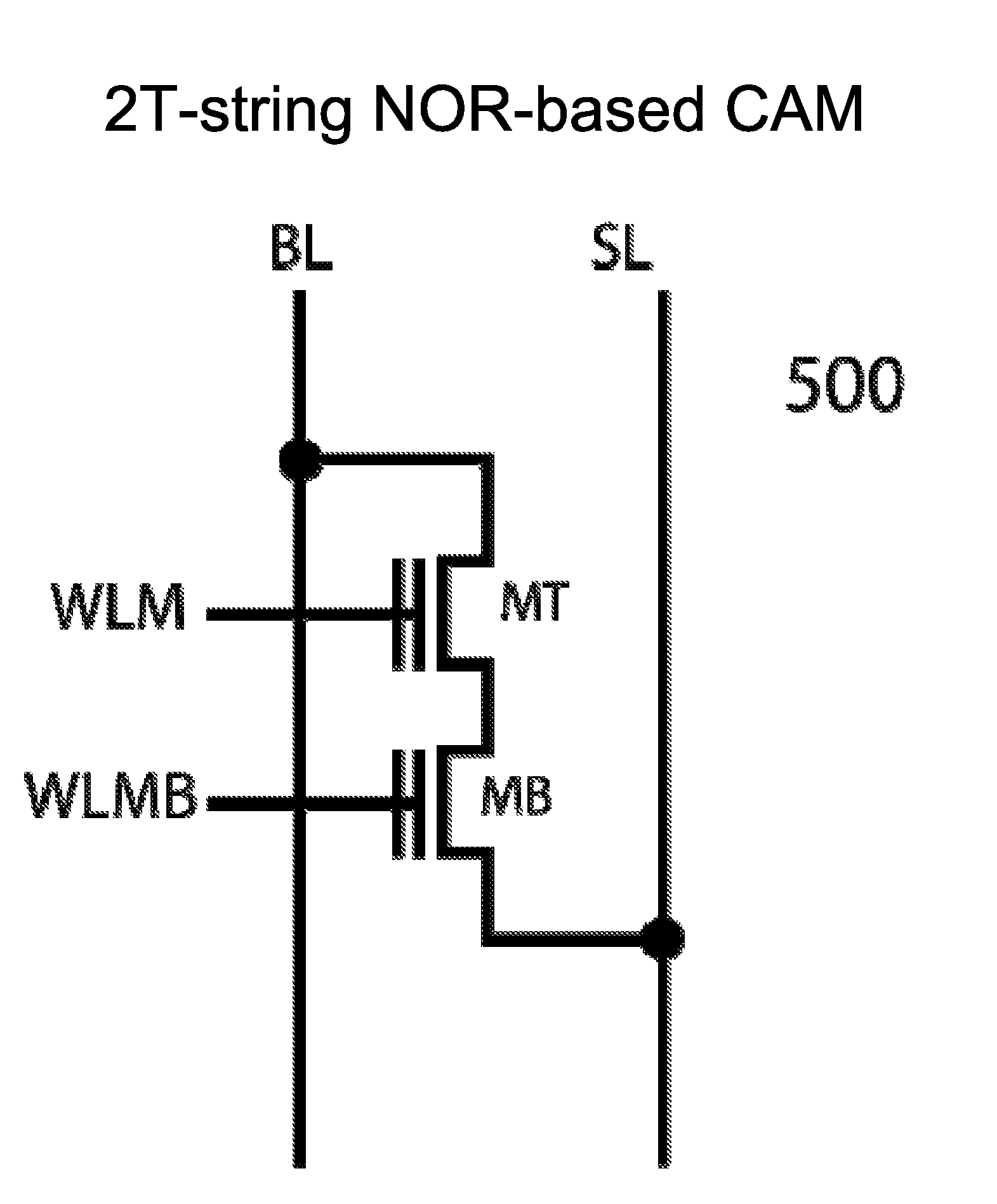
The present invention provides an extremely high-density non-volatile NOR-based BCAM or TCAM memory cell devices and arrays that achieve the high NAND-like cell scalability, low-power FN page write scheme, low-cost and non-volatile capability. The NOR-based BCAM and TCAM cell is designed to be faster and more flexible than the NAND-based CAM cell, and offers faster operations over both SRAM-based BCAM / TCAM cell and the DRAM-based BCAM / TCAM cell. One advantage of the NOR-based CAM cell is that it can be flexibly changed between BCAM and TCAM using the same number of flash transistors in one preferred sector of M×N 2T-string CAM cell vertical page and cell array of multiple vertical pages without adding any extra transistors for area saving. The speed of the NOR-based CAM cell is slower than the NAND-based CAM cell in a vertical page layout due to the lower number of contacts being used in the layout.

Problems solved by technology

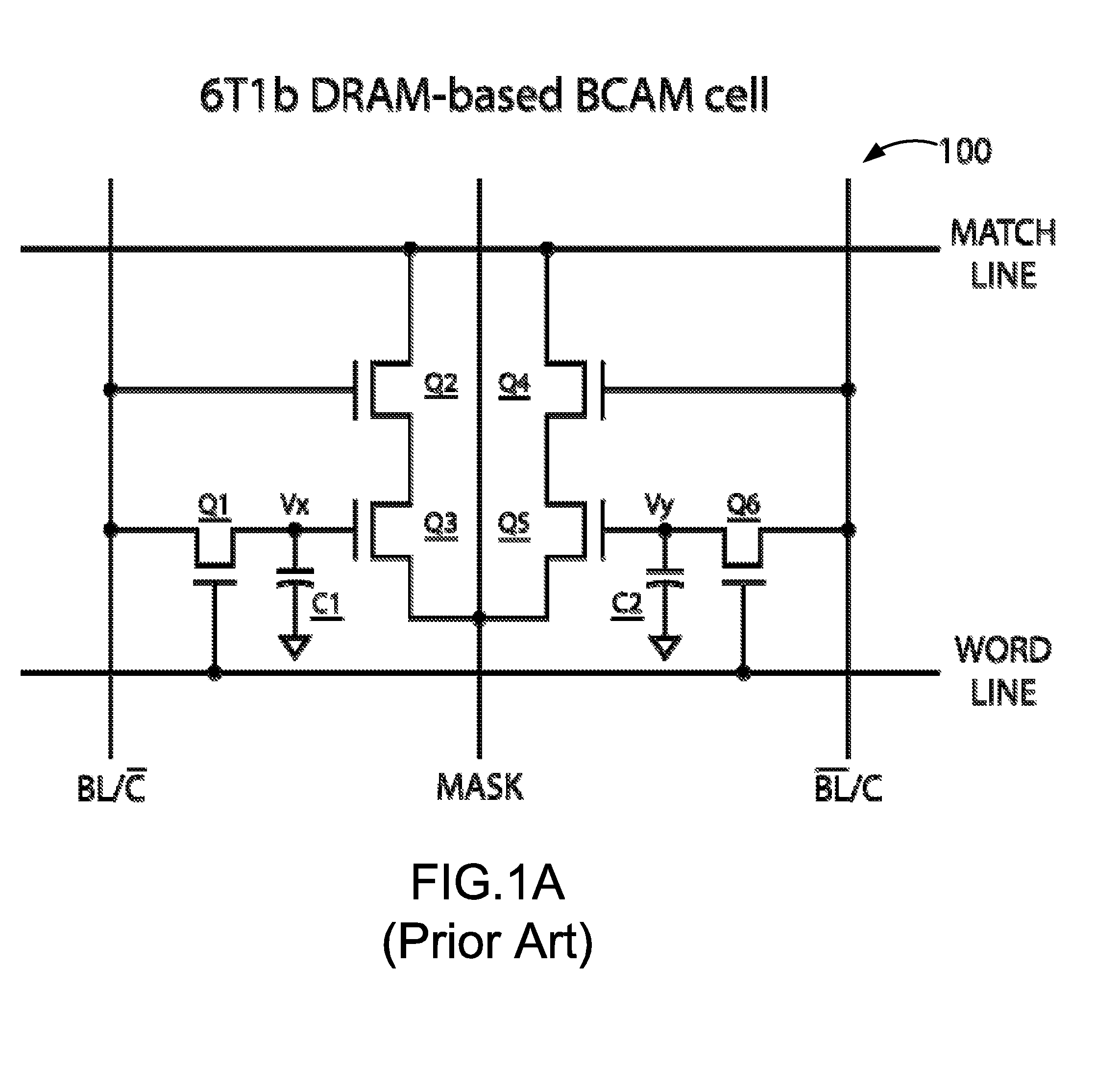
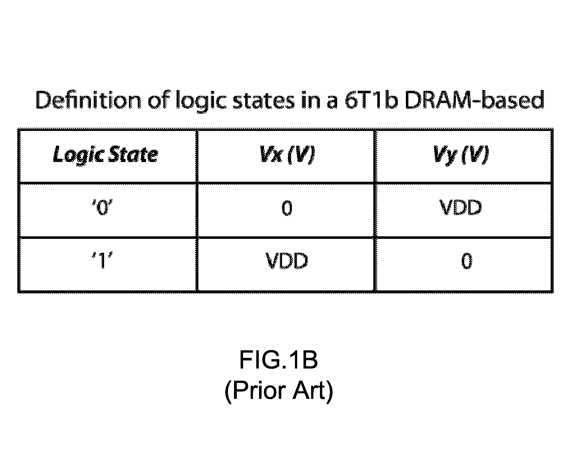
So far, the DRAM-based CAM has been gradually phased out in market place due to its disadvantageous need for its constant refresh-cycle that consumes too much power and is prone to data loss.
Conversely, the SRAM-based CAM does not require the refresh cycle to sustain its stored data but it suffers disadvantages of the big cell size and the risk of losing the VM stored data once the VDD power is removed.
But the disadvantage of the NAND-based CAM cell is the slow 20 μs Compare speed.
Both VM-based BCAM or TCAM cells are taking too much silicon area because it comprises two circuit parts.
But NVM NAND-based BCAM cannot be easily converted into NAND-based TCAM because the inherent cell string limitation.

Method used


Image

  • Nor-based bcam/tcam cell and array with NAND scalability
  • Nor-based bcam/tcam cell and array with NAND scalability
  • Nor-based bcam/tcam cell and array with NAND scalability

Examples


Embodiment Construction

[0061]In the following detailed description of the preferred embodiments, reference is made to the accompanying drawings, tables and flows that form a part hereof, and in which are shown by way of illustration specific preferred embodiments in which the inventions may be practiced. Basically, these embodiments will be described in sufficient detail to enable those skilled in the art to practice the invention, and it is to be understood that other embodiments may be utilized and that logical and electrical changes may be made without departing from the spirit and scope of the present invention.

[0062]The embodiments of the present invention cover one sector of non-volatile NOR-based BCAM and TCAM memory devices and arrays that comprises a plurality of 2T1b NAND cells. Both the Program and the Erase operations are substantially the same as the 2T2b NOR cell for Code storage in some patents granted to the same inventors and incorporated as references as indicated in the first section of...


PUM


Abstract

This invention discloses a 2T-string NOR-based CAM logic cell comprising two physical NAND cells connected in series with two horizontal WLs and one vertical BL and one vertical SL. Additionally, a sector of NOR-based CAM logic cell array is configured with N vertical cell strings each including M 2T-string NOR-based CAM logic cells connected in parallel sharing a local vertical SL and one dedicated vertical ML as an Operand word vertical page. Each 2T-string NOR-based CAM logic cell can be either a binary or ternary CAM cell associated with two or three physical states assigned to NAND cells' Vt levels for defining CAM logic states. Logic match of M-logic-bit inputs is found for at least one vertical page if the corresponding M 2T-string NOR-based CAM logic cells are in non-conduction state, providing M times faster Compare performance over the NAND-based CAM and 2 time faster than SRAM-based CAM.

Description

CROSS-REFERENCES TO RELATED APPLICATIONS[0001]This application claims priority to U.S. Provisional Patent Application No. 61 / 743,333, filed on Aug. 31, 2012, commonly assigned, and hereby incorporated by reference in its entirety herein for all purposes.[0002]Additionally, this application is related to U.S. Pat. Nos. 8,120,966, 8,120,959, 8,072,811, 7,688,612, 7,830,713, 8,233,320, 8,149,622, and U.S. patent application Ser. Nos. 13 / 135,220, 13 / 199,785, 13 / 199,527, 12 / 807,997, 61 / 275,148, 61 / 277,208, 61 / 574,632, and 61 / 687,227, commonly assigned, which are incorporated by reference herein for all purposes.[0003]This application is further related to a thesis paper of “Low-power High-performance Ternary Content Addressable Memory Circuits” presented by Mr. Nitin Moham to University of Waterloo, Ontario, Canada.[0004]Furthermore, this application is related to the following U.S. Pat. Nos. 7,848,129, 6,411,538, 6,567,340, 6,700,827, 7,016,211, 8,169,808, 8,031,502, 7,003,624, 6,256,21...

Claims


Application Information

Patent Timeline
IPC IPC(8): G11C15/04G11C16/04
CPCG11C16/0483G11C15/046G11C15/04
Inventor LEE, PETER WUNG
Owner APLUS FLASH TECH
Learn More