

Method of assembling vcsel chips on a sub-mount
a technology of vcsel chips and sub-mounts, which is applied in the direction of lasers, semiconductor lasers, solid-state devices, etc., can solve the problems of high cost and time consumption, and achieve the effect of high chip alignment accuracy
- Summary
- Abstract
- Description
- Claims
- Application Information
AI Technical Summary
Benefits of technology
Problems solved by technology
Method used
Image

Examples
Embodiment Construction
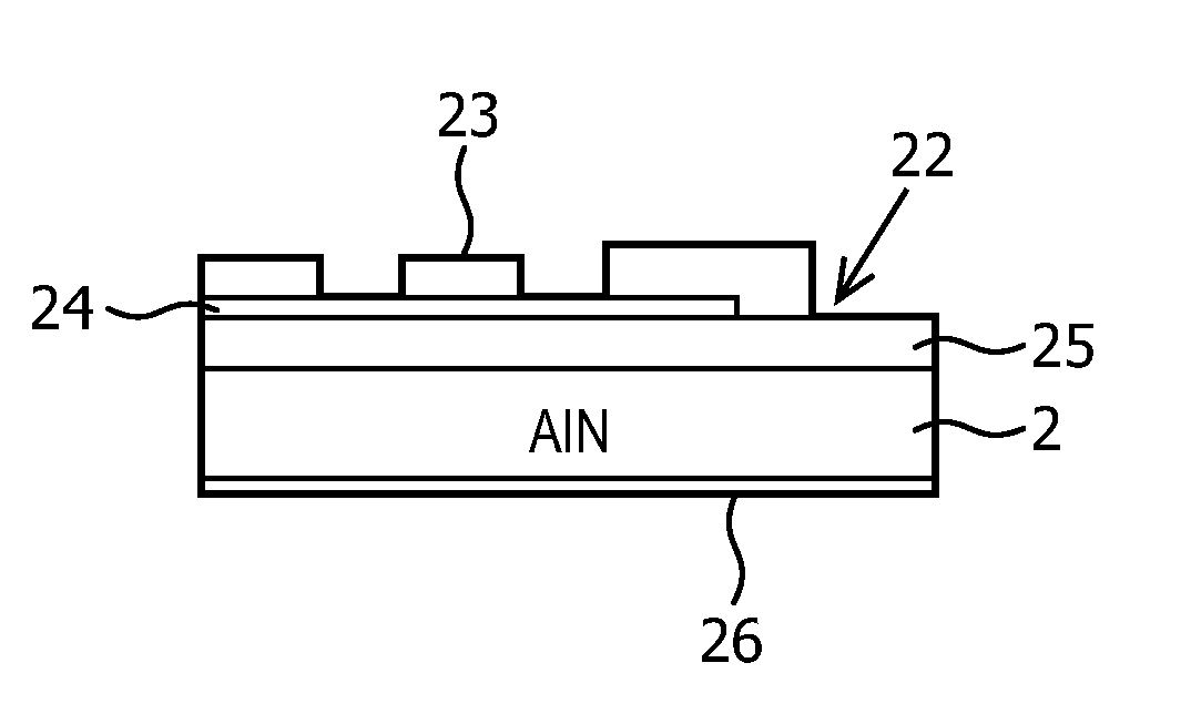
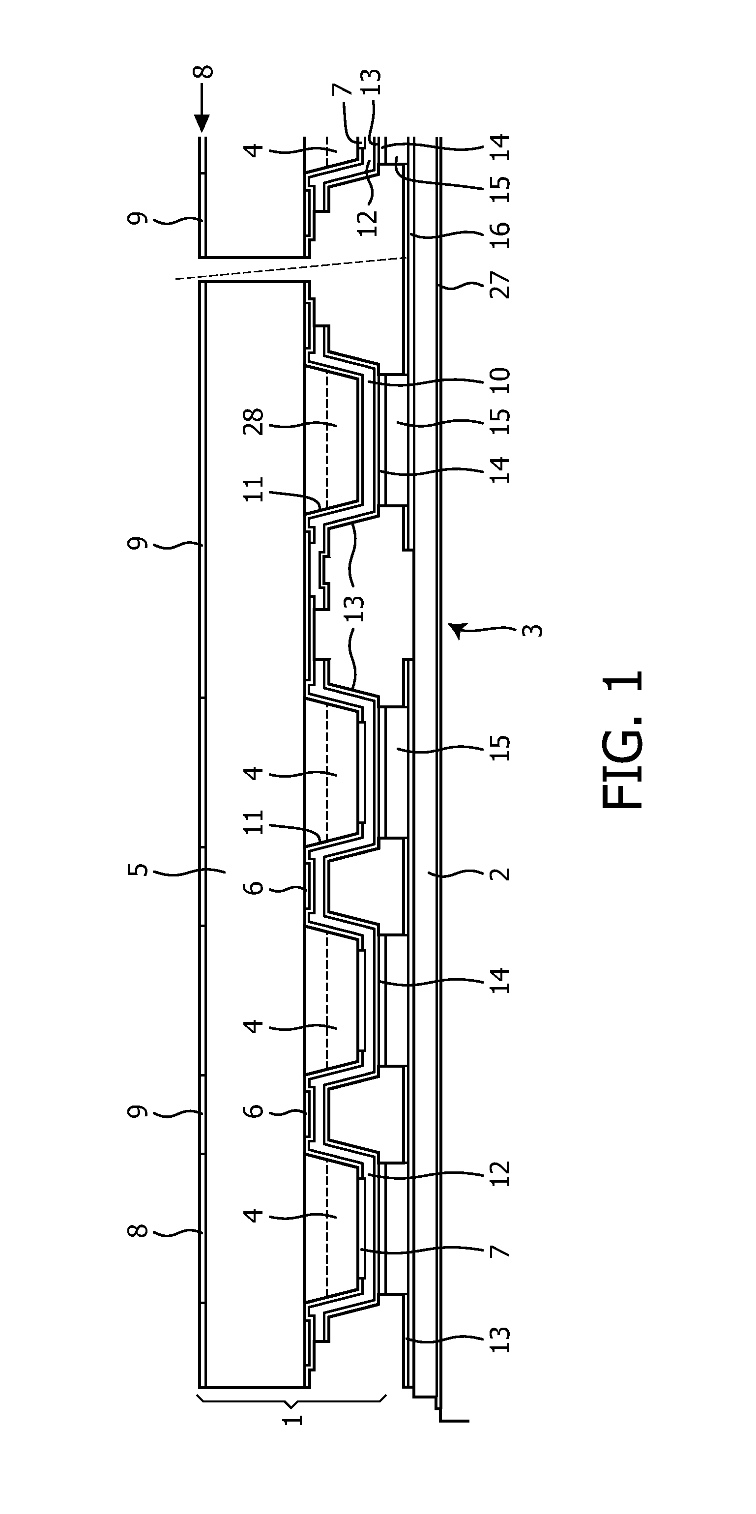
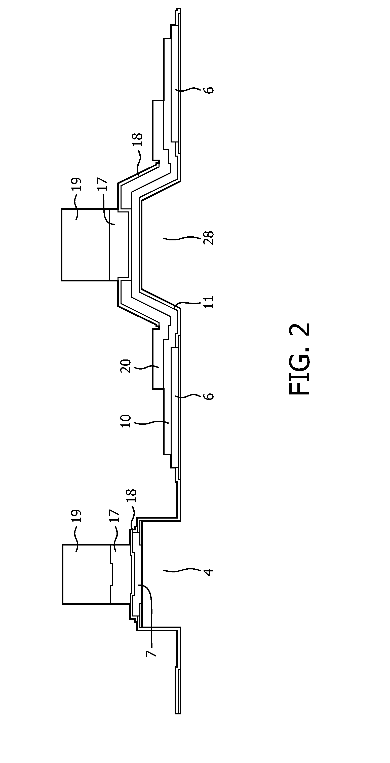
[0020]FIG. 1 shows an arrangement by which self alignment during soldering a bottom-emitter VCSEL chip 1 to a sub-mount 2 is achieved such that the emission windows of the VCSEL's of all chips on one sub-mount 2 are arranged in a desired exact manner with respect to each other. Each chip 1 comprises a VCSEL array of several VCSEL's from which three are shown with their p-type mesas 4 in FIG. 1. The figure shows the cross-section of one complete VCSEL chip 1 and only a small portion of a second chip at the right hand side. The VCSEL chips 1 comprise a n-type substrate 5 on which the p-type mesas 4 are formed in a known manner. The VCSEL's are connected by n-contacts 6 at the substrate side and p-contacts 7 on top of the mesas 4. The n-contacts 6 are metal layers having a low Ohmic contact (low Schottky barrier) to the n-type GaAs material of the substrate 5 or to the n-type DBR mirrors in case that mesa etching has stopped in these mirror layers (not shown in the figures). On the bot...
PUM
 Abstract
Description
Claims
Application Information